Freescale Semiconductor Data Sheet: Technical Data Document Number: MC13783 Rev. 3.5, 7/2009 MC13783 Package Information Plastic Package 10 × 10 mm package MC13783 Power Management and Audio Circuit 1 Introduction The MC13783 is a highly integrated power management and audio component dedicated to handset and portable applications covering GSM, GPRS, EDGE, and UMTS standards. The MC13783 implements high-performance audio functions suited to high-end applications such as smartphones and UMTS handsets.
Introduction The detailed block diagram of the MC13783 in Figure 1 shows the wide functionality of the MC13783, including the following features: • Battery charger interface for wall charging and USB charging • 10 bit ADC for battery monitoring and other readout functions • Buck switchers for direct supply of the processor cores • Boost switcher for backlight and USB on the go supply • Regulators with internal and external pass devices • Transmit amplifiers for two handset microphones and a headset microph
GNDSUB1 GNDSUB2 GNDSUB3 GNDSUB4 GNDSUB5 GNDSUB6 GNDSUB7 GNDSUB8 REFD REFC REFB REFA GNDATLAS VATLAS Tri-Color LED Drive Backlight LED Drive REFATLAS GNDLEDTC LOBATB LEDR3 LEDG3 LEDB3 LEDR2 LEDG2 LEDB2 GNDLEDBL LEDR1 LEDG1 LEDB1 LEDKP LEDAD1 LEDAD2 LEDMD1 LEDMD2 LEDMD3 LEDMD4 GNDCHRG CHRGLED CHRGSE1B CHRGMOD0 CHRGMOD1 CHRGRAW Charger Interface and Control: 4 bit DAC, Clamp, Protection, Trickle Generation Battery Interface & Protection BATTDETB CHRGCTRL BPFET CHRGISNSP CHRGISNSN
Introduction 1.1 Audio The audio section is composed of microphone amplifiers and speaker amplifiers, a voice CODEC, and a stereo DAC. Three microphone amplifiers are available for amplification of two handset microphones and of the headset microphone. The feedback networks are fully integrated for a current input arrangement. A line input buffer amplifier is provided for connecting external sources. All microphones have their own stabilized supply with an integrated microphone sensitivity setting.
Introduction regulators for the USB transceiver. The boost converter output has a backlight headroom tracking option to reduce overall power consumption. The regulators are directly supplied from the battery or from the switchers and include supplies for IO and peripherals, audio, camera, multi media cards, SIM cards, memory and the transceivers. Enables for external discrete regulators are included as well as a vibrator motor regulator.
Signal Descriptions 1.5 Miscellaneous Functions The drivers and comparators for a USB On-the-Go and a CEA-936-A compatible USB carkit including audio routing, as well as RS232 interfaces are provided. Special precautions are taken to allow for specific booting and accessory detection modes. Current sources are provided to drive tricolored funlights and signaling LEDs. The funlights have preprogrammed lighting patterns.
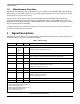
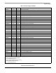
Signal Descriptions Table 1.
Signal Descriptions Table 1.
Signal Descriptions Table 1.
Signal Descriptions Table 1.
Signal Descriptions Table 1. Pinout Listing (continued) Pin VBUS Location Rating* D3 EHV EMV Function When in common input configuration, shorted to CHRGRAW 1. USB transceiver cable interface VBUS 2. Output VBUS regulator in USB on the go mode When in separate input configuration, not shorted to CHRGRAW 1. USB transceiver cable interface VBUS 2.
Signal Descriptions Table 1. Pinout Listing (continued) Pin Location Rating* Function Oscillator and Real Time Clock XTAL1 V16 LV 32.768 kHz Oscillator crystal connection 1 XTAL2 V14 LV 32.
Signal Descriptions Table 1.
Signal Descriptions Table 1.
Signal Descriptions Table 1. Pinout Listing (continued) Pin Location Rating* Function REFD L2 LV Reference for stereo DAC PLLLPF H2 LV Connection for the stereo DAC PLL low pass filter. GNDPLL H3 — Dedicated ground for the stereo DAC PLL block.
Electrical Characteristics 3 3.1 Electrical Characteristics Absolute Maximum Ratings Table 2 gives the maximum allowed voltages, current and temperature ratings which can be applied to the IC. Exceeding these ratings could damage the circuit. Table 2. Absolute Maximum Ratings Parameter 3.2 Min Typ Max Units Charger Input Voltage -0.3 — +20 V USB Input Voltage if Common to Charger -0.3 — +20 V USB Input Voltage if Separate from Charger -0.3 — +5.50 V Battery Voltage -0.3 — +4.
Functional Description 4 Functional Description 4.1 Logic The logic portions of the MC13783 includes the following: • Section 4.1.1, “Programmability,” on page 17 includes a description of the dual SPI interface. • Section 4.1.2, “Clock Generation and Real Time Clock,” on page 21 includes a description of the 32.768 kHz real time clock generation. • Section 4.1.3, “Power Control System,” on page 22 describes the power control logic, including interface and operated modes. 4.1.1 4.1.1.
Functional Description 4.1.1.2 Register Set The register set is given in Table 5. Table 5.
Functional Description The default CS polarity is active high. The CS line must remain active during the entire SPI transfer. In case the CS line goes inactive during a SPI transfer all data is ignored. To start a new SPI transfer, the CS line must go inactive and then go active again. The MISO line will be tri-stated while CS is low. Note that not all bits are truly writable. Refer to the individual subcircuit descriptions to determine the read/write capability of each bit.
Functional Description Tclkper CS Tclkhigh Tselsu Tclklow Tsellow Tselhld CLK Twrtsu Twrthld MOSI Trdsu Trden Trddis Trdhld MISO Figure 4. SPI Interface Timing Diagram Table 6.
Functional Description 4.1.2 4.1.2.1 Clock Generation and Real Time Clock Clock Generation The MC13783 generates a 32.768 kHz clock as well as several 32.768 kHz derivative clocks that are used internally for control. In addition, a 32.768 kHz square wave is output to external pins. 4.1.2.1.1 Clocking Scheme The MC13783 contains an internal RC oscillator powered from VATLAS that delivers a 32 kHz nominal frequency (±20%) at its output when an external 32.768 kHz crystal is not present.
Functional Description 4.1.3 Power Control System The power control system on MC13783 interfaces with the processors via different IO signals and the SPI bus. It also uses on-chip signals and detector outputs. It supports a system with different operating modes as described below. Table 8. MC13783 Operating Modes Mode Description Off Only the MC13783 core circuitry at VATLAS and the RTC module are powered. To exit the Off mode requires a turn on event.
Functional Description 4.2 4.2.1 Switchers and Regulators Supply Flow The switch mode power supplies and the linear regulators are dimensioned to support a supply flow based upon Figure 5.
Functional Description Table 9. Regulator Output Voltages (continued) Supply Output (V) Load (mA) VIOLO 1.2/1.3/1.5/.18 150 (Vout < 1.5V)/200 (Vout ≥ 1.5V) VDIG 1.2/1.3/1.5/.18 150 (Vout < 1.3V)/200 (Vout ≥ 1.3V) VRFDIG 1.2/1.5/1.8/1.875 150 (Vout < 1.8V)/200 (Vout ≥ 1.8V) VGEN 1.1/1.2/1.3/1.5/1.8/2.0/2.4/2.775 150 (Vout < 1.5V)/200 (Vout ≥ 1.5V) VCAM 1.5/1.8/2.5/2.55/2.6/2.75/2.8/3.0 150 VRFBG 1.250 0.1 VRFREF 2.475/2.600/2.700/2.775 50 VRFCP 2.700/2.775 50 VSIM 1.8/2.
Functional Description Table 10. Regulator General Characteristics (continued) Parameter Condition Min Typ Max Units Minimum Bypass Capacitor Value Used as a condition for all other parameters. -35% 2.2 +35% µF Minimum Bypass Capacitor Value for: VRFREF, VRFCP, VIOHI, VSIM, VESIM Used as a condition for all other parameters. -35% 1 — µF Bypass Capacitor Value for VAUDIO Used as a condition for all other parameters.
Functional Description 4.3 4.3.1 4.3.1.1 Audio Dual Digital Audio Bus Interface The MC13783 is equipped with two independent digital audio busses. Both busses consist of a bit clock, word clock, receive data and transmit data signal lines. Both busses can be redirected to either the voice CODEC or the stereo DAC and can be operated simultaneously. In addition to the afore mentioned signal lines, two system clock inputs are provided which can be selected to drive the voice CODEC or the stereo DAC.
Functional Description DAC will operate in its assigned time slot. A total of maximum 4 time slot pairs are supported depending on the settings of the clock speed. In this case, the sync signal is no longer a word select but a short frame sync. In all modes, the polarity of both FS and BCL is programmable by SPI. There is also the possibility to activate the clocking circuitry independent from the stereo DAC. 4.3.1.
Functional Description Table 13. Telephone CODEC D/A Performance Specifications Parameter Condition Peak Output (+3 dBm0) single ended output Min Typ REFC - 1 Max Units REFC + 1 V CODEC PSRR with respect to B+, 20 Hz to 20 kHz, 80 90 — dB Total Distortion (noise and harmonic) at 1.02 kHz, 0 dBm0, 20 kHz measurement BW out 65 75 — dB Idle Channel Noise at CODEC output, BW out = 20 kHz A weighted — -78 -74 dBm0 Inband Spurious 0 dBm0 at 1.02 kHz to 3.4 kHz input. 300 Hz to 20.
Functional Description 4.3.3.2 Clock Modes The stereo DAC incorporates a PLL to generate the proper clocks in master and in slave modes. The PLL requires an external C//RC loop filter. In Master Mode, the PLL of the Stereo DAC generates FS and BCL signal based on the reference frequency applied through one of the CLI inputs. The CLI frequencies supported are 3.6864 MHz, 12 MHz, 13 MHz, 15.36 MHz, 16.8 MHz, 26 MHz and 33.6 MHz.
Functional Description Table 15. Stereo DAC Sample Rate Selection SPI Bits (continued) SR3 SR2 SR1 SR0 FS NFS MCL NB BCL 1 0 0 0 48000 128 6144k 4 1536k 1 0 0 1 64000 64 4096k 2 2048k 1 0 1 0 96000 64 6144k 2 3072k 1011 to 1111 are reserved combinations 4.3.4 Audio Input Section 4.3.4.1 Microphone Bias Two microphone bias circuits are provided. One circuit supplies up to two handset microphones via the two outputs MC1RB and MC1LB.
Functional Description Detect Microphone Bias PGAtxL MC2B Rbias MC1RB Rbias MC1LB MC1LIN Amc1L Input Selector PGAtxL Rbias From RXINL Voice Codec Amc1R Input Selector PGAtxR MC1RIN MC2IN Amc2 PGAtxR Atxin To Rx From RXINR TXIN TXOUT From USB Figure 8. Audio Input Section Diagram Table 17. Amplifiers Amc1L, Amc1R, Amc2, Atxin Performance Specifications Parameter Condition Vin = 100 mVpp Min Typ Max Units 11.8 12 12.2 dB Gain (V to V) at 1.
Functional Description 4.3.5 Audio Output Section 4.3.5.1 Audio Signal Routing Figure 9 on page 32 shows a block diagram of the audio output section is given indicating the routing possibilities.
Functional Description 4.3.5.2 Programmable Gain Amplifiers The gain of the audio in both left and right channels is independently controlled in the programmable gain amplifiers to allow for balance control. The input level from the external stereo source can be pre-amplified by Arxin of 18 dB and the programmable gain amplifier PGArxin to get it at the same level as the other sources before going into the audio input mixer block. The amplifiers are programmable in 3 dB steps from –33 dB to +6 dB. 4.3.
Functional Description 4.3.5.5 Loudspeaker Amplifier Alsp The concept of the Alsp amplifier is especially developed to be able to drive one loudspeaker during handset, speakerphone and alert modes. It adopts a fully differential topology in order to be able to reach high PSRR performance while Alsp is powered directly by the telephone battery. The feedback network of the Alsp amplifier is fully integrated. Under worst case conditions the dissipation of Alsp is considerable.
Functional Description Table 20. Amplifiers Ahsr and Ahsl Performance Specifications (continued) Parameter THD (2nd and 3rd) Condition 1.0 kHz Min Typ Max Units VOUT = 1 VPP — 0.03 0.1 % VOUT = 10 mVRMS — 0.03 0.1 % PSRR with respect to BP 20 Hz - 20 kHz inputs AC grounded A Weighted 90 — — dB Input Noise A weighted — — 20 μVRMS Load Impedance Resistance 12.
Functional Description 4.3.6 4.3.6.1 Audio Control Supply The audio section is supplied from a dedicated regulator VAUDIO, except for the loudspeaker amplifier Alsp which is directly supplied from the battery. A low power standby mode controlled by the standby pins is provided for VAUDIO in which the bias current is reduced. The output drive capability and performance are limited in this mode. The nominal output voltage for VAUDIO is 2.775 V.
Functional Description Table 22. Charger Mode Selection (continued) 4.4.1.1 CHRGMOD1 CHRGMOD0 Charger Mode VATLAS GND Separate Input Dual Path VATLAS Hi Z Separate Input Single Path VATLAS VATLAS Separate Input Serial Path GND GND Reserved GND Hi Z Reserved GND VATLAS Reserved Serial Path Configuration Example In serial path configuration, the current path used for charging the battery is the same as the supply path from charger to radio B+.
Functional Description Table 23. Voltage and Current Settings Parameter Set Points Regulated charge voltage at BP Programmable voltage setting of 3.80/4.05/4.15/4.20/4.25/4.30/4.375/4.50V. Regulated charge current through M1M2 Programmable current from 0 to 1600 mA in 14 steps, and fully on mode. Internal trickle charge current Programmable current from 0 to 84mA in steps of 12mA. 4.4.1.2 4.4.1.2.
Functional Description provide the leakage current of the coin cell. The RTC will run from VATLAS in this case. A capacitor should be placed from LICELL to ground if no coin cell is used. 4.4.2 ADC Subsystem 4.4.2.1 Converter Core The ADC core is a 10 bit successive approximation converter. 4.4.2.2 Input Selector The ADC has two groups of 8 input channels. ADSEL selects between two groups of input signals. If set to zero then group 0 is read and stored, if set to 1 then group 1 is read and stored.
Functional Description 4.4.2.3 Control The ADC parameters are programmed by the processors via SPI. Locally on MC13783, the different ADC requests are arbitrated and executed. When a conversion is finished, an interrupt is generated to the processor which started the conversion. 4.4.2.3.1 Starting Conversions The ADC will have the ability to start a series of conversions based on a rising edge of the ADTRIG signal or directly initiated by SPI.
Functional Description 4.4.2.5.4 Die Temperature and UID The die temperature can be read out on the ADIN7 channel. Alternatively, the UID voltage can be read out on the ADIN7 channel. 4.4.2.6 Touch Screen Interface The touchscreen interface provides all circuitry required for the readout of a 4-wire resistive touchscreen. The touchscreen X plate is connected to TSX1 and TSX2 while the Y plate is connected to TSY1 and TSY2. A local supply ADREF will serve as a reference.
Functional Description 4.4.2.7 ADC Arbitration The ADC converter and its control is based on a single ADC converter core. Since the data path is 24 bits wide, results for 2 conversion results (10 bits each) can be read back in each SPI read sequence. For support of queued conversion requests, the SPI has the ability to write to the two sets of ADC control, namely “its own” ADC and “the other” ADC or ADC BIS.
UDATVP UDP Tx USE0VM UDM TO ACCESSORY CONNECTOR Functional Description TO PROCESSOR Router SEO UTXENB URXVP Rx URCVD Diff URXVM Rx DATSEO, BIDIR Figure 11. USB/RS232 Transceiver Data Flow Upon a USB legacy host detection, an interrupt is generated but neither the transceiver nor the VUSB regulator are automatically enabled. This must be done by software before data transmission. The transceiver can also be enabled during boot mode.
Functional Description Table 26.
Functional Description An ID detector is used to determine if a mini-A or mini-B style plug has been inserted into a mini-AB style receptacle on the phone. The ID voltage can be read out via the ADC channel ADIN7. 4.5.1.2 RS-232 Interface In RS232 mode, USBVCC is used for the supply of the interface with the microprocessor. VUSB is used as the supply for the RS232 transceiver and the drivers at the cable side.
Functional Description BOOST Key Pad BOOST Main Display Aux Display BOOST P B 1 D M D E L 2 D M D E L 3 D M D E L 4 D M D E L BL Drive Main Display 1 D A D E L 2 D A D E L BL Drive Aux Display P K D E L L B D E L D N G BL Drive Keypad 1 R D E L 1 G D E L BOOST P B 1 B D E L 2 R D E L 2 G D E L BOOST P B 2 B D E L 3 R D E L 3 G D E L 3 B D E L C T D E L D N G Tri-Color Fun Light Drive MC13783 IC Lighting System Figure 12. MC13783 Lighting System 4.5.2.
Package Information supply such as the on-chip boost switcher should be used to ensure adequate headroom if necessary, such as for driving blue LEDs. The channel naming assignments are R, G, and B representative of applications which use red, green, and blue colored LEDs on each of the respective zones. One set of RGB drivers constitute a tri-color bank, and the MC13783 features three tri-color banks. Each tri-color LED driver is programmable for independent control of timing and current levels.
Product Documentation 6 Product Documentation This data sheet is labeled as a particular type: Product Preview, Advance Information, or Technical Data. Definitions of these types are available at: http://www.freescale.com on the Documentation page. Table 27 summarizes revisions to this document since the previous release (Rev. 3.4). Table 27. Revision History Location Revision Table 1 Change SW3IN to HV in Table 1. Table 3 Updated consumption numbers in Table 3.
NOTES MC13783 Technical Data, Rev. 3.
How to Reach Us: Home Page: www.freescale.com Web Support: http://www.freescale.com/support USA/Europe or Locations Not Listed: Freescale Semiconductor Technical Information Center, EL516 2100 East Elliot Road Tempe, Arizona 85284 +1-800-521-6274 or +1-480-768-2130 www.freescale.