
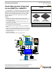
Datasheet

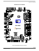

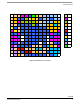


PIN CONNECTIONS
Analog Integrated Circuit Device Data
10 Freescale Semiconductor
MC13892
M4 M5 VSRTC 3.6 Output SRTC Supply
Output regulator for SRTC module on
processor
M5 P6 GNDRTC – Ground Real Time Clock
Ground
Ground for the RTC block
M6 M7 VINCAMDRV 5.5 I/O Camera Regulator
Supply Input and Driver
Output
1. Input regulator camera using internal
PMOS FET.
2. Drive output regulator for camera voltage
using external PNP device.
M7 N8 PWGTDRV2 4.8 Output Power Gate Driver 2
Power gate driver 2
M8 L9 VDIG 3.6 Output Digital Supply
Output regulator digital
M9 P11 VINDIG 5.5 Input VDIG Supply Input
Input regulator digital
M10 M10 VGEN1DRV 5.5 Output VGEN1 Driver
Drive output GEN1 regulator
M11 N13 ADIN7 4.8 Input ADC Channel 7 Input
ADC generic input channel 7, group 1
M12 M14 TSY1 3.6 Input Touch Screen
Interface Y1
Touch screen interface Y1
M13, N12,
N13
N14 TSREF 3.6 Output Touch Screen
Reference
Touch screen reference
N3 M2 VINGEN3DRV 5.5 Power/Output VGEN3 Supply Input
and Driver Output
1. Input VGEN3 regulator
2. Drive VGEN3 output regulator
N4 P4 VGEN2DRV 5.5 Output VGEN2 Driver
Drive output GEN2 regulator
N5 N5 XTAL2 2.5 Input Crystal Connection 2
32.768 kHz oscillator crystal connection 2
N6 N6 XTAL1 2.5 Input Crystal Connection 1
32.768 kHz oscillator crystal connection 1
N7 L8 VINAUDIO 5.5 Power Audio Supply Input
Input regulator VAUDIO
N8 N7 VAUDIO 3.6 Output Audio Supply
Output regulator for audio
N9 N9 VIOHI 3.6 Output High Voltage IO Supply
Output regulator high voltage IO, efuse
N10 N10 VINIOHI 5.5 Input High Voltage IO Supply
Input
Input regulator high voltage IO
N11 M11 VGEN1 3.6 Output General Purpose
Regulator 1
Input GEN1 regulator
Table 2. MC13892 Pin Definitions (continued)
A functional description of each pin can be found in the Functional Description.
Pin Number
on the
13982VK
7x7 mm
Pin Number on
the 13982VL
12x12 mm
Pin Name
Rating
(V)
Pin Function Formal Name Definition