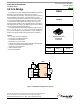
Freescale Semiconductor Technical Data Document Number: MC33886 Rev 9.0, 4/2011 5.0 A H-Bridge 33886 The 33886 is a monolithic H-Bridge ideal for fractional horsepower DC-motor and bi-directional thrust solenoid control. The IC incorporates internal control logic, charge pump, gate drive, and low RDS(ON) MOSFET output circuitry. The 33886 is able to control continuous inductive DC load currents up to 5.0 A. Output loads can be pulse width modulated (PWM-ed) at frequencies up to 10 kHz.
INTERNAL BLOCK DIAGRAM INTERNAL BLOCK DIAGRAM C VPWR CCP V+ CP Charge Pump 80 μA 80 uA (each) OUT1 IN1 IN2 D1 D2 Current Limit, Current Limit, Overcurrent Short-circuit Sense Sense Circuit Circuit 5.0 V Regulator Gate Drive OUT2 25 uA 25 μA Control Logic OverOvertemperature temperature Under-voltage Undervoltage FS AGND PGND Figure 2.
PIN CONNECTIONS PIN CONNECTIONS AGND 1 20 DNC FS 2 19 IN2 IN1 3 18 D1 V+ 4 17 CCP V+ 5 16 V+ OUT1 6 15 OUT2 OUT1 7 14 OUT2 DNC 8 13 D2 PGND 9 12 PGND PGND 10 11 PGND Figure 3. 33886 Pin Connections Table 1. 33886 Pin Definitions A functional description of each pin can be found in the Functional Pin Description section beginning on page 15.
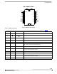
ELECTRICAL CHARACTERISTICS MAXIMUM RATINGS ELECTRICAL CHARACTERISTICS MAXIMUM RATINGS Table 2. Maximum Ratings All voltages are with respect to ground unless otherwise noted. Exceeding these ratings may cause a malfunction or permanent damage to the device. Rating Supply Voltage Input Voltage (1) FS Status Output (2) Continuous Current (3) Symbol Value Unit V+ 40 V VIN -0.1 to 7.0 V V FS 7.0 V IOUT 5.
ELECTRICAL CHARACTERISTICS STATIC ELECTRICAL CHARACTERISTICS STATIC ELECTRICAL CHARACTERISTICS Table 3. Static Electrical Characteristics Characteristics noted under conditions 5.0 V ≤ V+ ≤ 28 V and -40°C ≤ TA ≤ 125 °C, unless otherwise noted. Typical values noted reflect the approximate parameter mean at TA = 25 °C under nominal conditions, unless otherwise noted. Characteristic Symbol Min Typ Max Unit V+ 5.
ELECTRICAL CHARACTERISTICS STATIC ELECTRICAL CHARACTERISTICS Table 3. Static Electrical Characteristics Characteristics noted under conditions 5.0 V ≤ V+ ≤ 28 V and -40°C ≤ TA ≤ 125 °C, unless otherwise noted. Typical values noted reflect the approximate parameter mean at TA = 25 °C under nominal conditions, unless otherwise noted. Characteristic Symbol Min Typ Max Unit POWER OUTPUTS (OUT1, OUT2) Output-ON Resistance (13) RDS(ON) mΩ 5.0 V ≤ V+ ≤ 28 V, TJ = 25 °C – 120 – 8.
ELECTRICAL CHARACTERISTICS DYNAMIC ELECTRICAL CHARACTERISTICS DYNAMIC ELECTRICAL CHARACTERISTICS Table 4. Dynamic Electrical Characteristics Characteristics noted under conditions 5.0 V ≤ V+ ≤ 28 V and -40°C ≤ TA ≤ 125 °C, unless otherwise noted. Typical values noted reflect the approximate parameter mean at TA = 25 °C under nominal conditions, unless otherwise noted.
ELECTRICAL CHARACTERISTICS TIMING DIAGRAMS VIN1, IN2 (V) TIMING DIAGRAMS 5.0 50% VOUT1, 2 (V) 0 50% td(OFF) td(ON) VPWR 90% 10% 0 TIME Figure 4. Output Delay Time 5.0 V 0V ℘?ℜ 0Ω VOUT1, 2 (V) Figure 5. Disable Delay Time V PWR tf tr 90% 90% 10% 10% 0 IIMAX CURRENT (A) (A) LIM, IOUTPUT LIM, CURRENT Figure 6. Output Switching Time 6.5 6.6 2.5 Thermal Shutdown 160 175 T J, JUNCTION TEMPERATURE (o C) Figure 7.
ELECTRICAL CHARACTERISTICS TIMING DIAGRAMS Diode Reverse FS, SF LOGIC OUT D2, LOGIC IN D1, LOGIC IN INn, LOGIC IN IOUT , CURRENT (A) (A) CURRENT IILOAD ,, OUTPUT OUT Spikes LoadRecovery Capacitance and/or Diode Reverse Recovery Spikes 8.0 ISCL Short-circuit Detect Threshold Typ. Short Ckt. Detect Threshold 6.5 Typical Current Threshold Typ.
ELECTRICAL CHARACTERISTICS TYPICAL SWITCHING WAVEFORMS TYPICAL SWITCHING WAVEFORMS • • • • Important For all plots, the following applies: Ch2 = 2.0 A per division LLOAD = 533 μH @ 1.0 kHz LLOAD = 530 μH @ 10.0 kHz RLOAD = 4.0 Ω Output Voltage (OUT1) IOUT Output Voltage (OUT1) Input Voltage (IN1) V+=34 V IOUT fPWM =1.0 kHz Duty Cycle=90% Figure 12. Output Voltage and Current vs. Input Voltage at V+ = 34 V, PMW Frequency of 1.
ELECTRICAL CHARACTERISTICS TYPICAL SWITCHING WAVEFORMS Output Voltage (OUT1) Output Voltage (OUT1) IOUT IOUT Input Voltage (IN1) Input Voltage (IN1) V+=24 V fPWM =10 kHz V+=12 V Duty Cycle=50% Figure 14. Output Voltage and Current vs. Input Voltage at V+ = 24 V, PMW Frequency of 10 kHz, and Duty Cycle of 50% Output Voltage (OUT1) IOUT IOUT Input Voltage (IN1) Input Voltage (IN1) fPWM =10 kHz Duty Cycle=90% Figure 15. Output Voltage and Current vs.
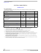
ELECTRICAL CHARACTERISTICS TYPICAL SWITCHING WAVEFORMS Table 5. Truth Table The tri-state conditions and the fault status are reset using D1 or D2. The truth table uses the following notations: L = Low, H = High, X = High or Low, and Z = High-impedance (all output power transistors are switched off).
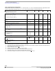
ELECTRICAL CHARACTERISTICS ELECTRICAL PERFORMANCE CURVES ELECTRICAL PERFORMANCE CURVES 0.40 0.35 0.30 Ohms 0.25 0.20 0.15 0.10 0.05 0.0 5 7 9 11 13 15 17 19 21 23 25 27 29 31 33 35 37 39 41 Volts Figure 18. Typical High Side RDS(ON) Versus V+ 0.13 Ohms OHMS 0.128 0.126 0.124 0.122 0.12 5 7 9 11 13 15 17 19 21 23 25 27 29 31 33 35 37 39 41 Volts VPWR Figure 19.
ELECTRICAL CHARACTERISTICS ELECTRICAL PERFORMANCE CURVES 9.0 8.0 7.0 milliOHMS amperes 6.0 5.0 4.0 3.0 2.0 1.0 0.0 5 7 9 11 13 15 17 19 21 23 25 27 29 31 33 35 37 39 41 Volts VPWR Figure 20.
FUNCTIONAL DESCRIPTION INTRODUCTION FUNCTIONAL DESCRIPTION INTRODUCTION Numerous protection and operational features (speed, torque, direction, dynamic braking, and PWM control), in addition to the 5.0 A current capability, make the 33886 a very attractive, cost-effective solution for controlling a broad range of fractional horsepower DC motors. A pair of 33886 devices can be used to control bipolar stepper motors in both directions.
FUNCTIONAL DESCRIPTION FUNCTIONAL PIN DESCRIPTION H-BRIDGE OUTPUT 1, 2 (OUT1 AND OUT2) These pins are the outputs of the H-Bridge with integrated output FET body diodes. The bridge output is controlled using the IN1, IN2, D1, and D2 inputs. The outputs have active current limiting above 6.5 A. The outputs also have thermal shutdown (tri-state latch-OFF) with hysteresis as well as short-circuit latch-OFF protection.
FUNCTIONAL DEVICE OPERATION FUNCTIONAL PIN DESCRIPTION FUNCTIONAL DEVICE OPERATION SHORT-CIRCUIT PROTECTION If an output short-circuit condition is detected, the power outputs tri-state (latch-OFF) independent of the input (IN1 and IN2) states, and the fault status output flag is set logic Low.
FUNCTIONAL DEVICE OPERATION PERFORMANCE PERFORMANCE The 33886 is designed for enhanced thermal performance. The significant feature of this device is the exposed copper pad on which the power die is soldered. This pad is soldered on a PCB to provide heat flow to ambient and also to provide thermal capacitance. The more copper area on the PCB, the better the power dissipation and transient behavior will be. Example Characterization on a double-sided PCB: bottom side area of copper is 7.
TYPICAL APPLICATIONS TYPICAL APPLICATIONS A typical application schematic is shown in Figure 23. For precision high-current applications in harsh, noisy environments, the V+ by-pass capacitor may need to be substantially larger. DC MOTOR V+ 33886 AGND V+ CCP OUT1 33 nF + 47 μF OUT2 D2 D1 FS PGND IN1 IN2 IN2 IN1 FS D1 D2 Figure 23.
PACKAGING PACKAGE DIMENSIONS PACKAGING PACKAGE DIMENSIONS Important For the most current revision of the package, visit www.freescale.com and perform a keyword search on 98ASH70702A listed.
PACKAGING PACKAGE DIMENSIONS VW (Pb-FREE) SUFFIX 20-PIN HSOP 98ASH70702A ISSUE B 33886 Analog Integrated Circuit Device Data Freescale Semiconductor 21
PACKAGING PACKAGE DIMENSIONS VW (Pb-FREE) SUFFIX 20-PIN HSOP 98ASH70702A ISSUE B 33886 22 Analog Integrated Circuit Device Data Freescale Semiconductor
5.0 A H-BRIDGE THERMAL ADDENDUM - REVISION 2.0 5.0 A H-BRIDGE 33886HSOP THERMAL ADDENDUM - REVISION 2.0 Introduction This thermal addendum is provided as a supplement to the MC33186 technical data sheet. The addendum provides thermal performance information that may be critical in the design and development of system applications. All electrical, application, and packaging information is provided in the data sheet.
5.0 A H-BRIDGE THERMAL ADDENDUM - REVISION 2.0 A AGND FS IN1 V+ V+ OUT1 OUT1 DNC PGND PGND 1 2 3 4 5 6 7 8 9 10 20 19 18 17 16 15 14 13 12 11 DNC IN2 D1 CCP V+ OUT2 OUT2 D2 PGND PGND 33886 Pin Connections 20-Pin HSOP 1.27 mm Pitch 16.0 mm x 11.0 mm Body 12.2 mm x 6.9 mm Exposed Pad Figure 25. Thermal Test Board Device on Thermal Test Board Material: Outline: Single layer printed circuit board FR4, 1.6 mm thickness Cu traces, 0.
Thermal Resistance [ºC/W] 5.0 A H-BRIDGE THERMAL ADDENDUM - REVISION 2.0 60 50 40 30 x RθJA 20 10 0 0 300 Heat spreading area A [mm²] 600 Figure 26. Device on Thermal Test Board RθJA Thermal Resistance [ºC/W] 100 x RθJA 10 1 0.1 1.00E-03 1.00E-02 1.00E-01 1.00E+00 1.00E+01 1.00E+02 1.00E+03 1.00E+04 time[s] Time(s) Figure 27.
REVISION HISTORY REVISION HISTORY REVISION DATE DESCRIPTION OF CHANGES 7.0 7/2005 • • • Implemented Revision History page Added Thermal Addendum Converted to Freescale format 8.0 2/2007 • • Updated data sheet format Removed Peak Package Reflow Temperature During Reflow (solder reflow) parameter from Maximum Ratings on page 4. Added note with instructions to obtain this information from www.freescale.com. 9.
How to Reach Us: Home Page: www.freescale.com Web Support: http://www.freescale.com/support USA/Europe or Locations Not Listed: Freescale Semiconductor, Inc. Technical Information Center, EL516 2100 East Elliot Road Tempe, Arizona 85284 +1-800-521-6274 or +1-480-768-2130 www.freescale.