
Datasheet


Analog Integrated Circuit Device Data
11 Freescale Semiconductor
34709
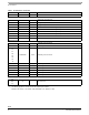
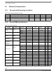
Pin Connections
A3 GNDSPI GND
Ground for SPI interface
A to D Converter
H6 ADIN9 I
ADC generic input channel 9
J5 ADIN10 I
ADC generic input channel 10
J6 ADIN11 I
ADC generic input channel 11
K5 TSX1 I
Touch Screen Interface X1 or ADC generic input channel 12
L4 TSX2 I
Touch Screen Interface X2 or ADC generic input channel 13
L6 TSY1 I
Touch Screen Interface Y1 or ADC generic input channel 14
L3 TSY2 I
Touch Screen Interface Y2 or ADC generic input channel 15
K6 TSREF O
Touch screen reference
H5 GNDADC GND
Ground for A to D circuitry
Substrate Grounds
K8 SUBSREF GND
Substrate ground connection
K9 SUBSPWR GND
Substrate ground connection
E8
F8
F9
G8
G9
H8
H9
J9
SUBSPWR1 GND
Substrate ground connection
E11 SUBSPWR2 GND
Substrate ground connection
G10 SUBSPWR3 GND
Substrate ground connection
H10 SUBSLDO GND
Substrate ground connection
K12 SUBSANA1 GND
Substrate ground connection
F10 SUBSANA2 GND
Substrate ground connection
J8 SUBSGND GND
Substrate ground connection
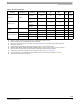
No connects
A14
B15
R1
NC -
Do not connect
Notes
2. If a switching regulator is not used, connect the regulator pins as follows:
SWxVIN = BP, SWxLX = NC, SWxFB = GND, SWxPWGD = NC, SWxCFG = GND
Table 3. Pin Definitions (continued)
Pin Number Pin Name Pin Function Definition