
Datasheet


Analog Integrated Circuit Device Data
13 Freescale Semiconductor
34709
General Product Characteristics
5.2 Thermal Characteristics
The thermal rating data of the packages has been simulated with the results listed in Table 5.
Junction to Ambient Thermal Resistance Nomenclature: the JEDEC specification reserves the symbol R
θJA
or θJA (Theta-JA)
strictly for junction-to-ambient thermal resistance on a 1s test board in natural convection environment. R
θJMA
or θJMA
(Theta-JMA) will be used for both junction-to-ambient on a 2s2p test board in natural convection and for junction-to-ambient with
forced convection on both 1s and 2s2p test boards. It is anticipated that the generic name, Theta-JA, will continue to be commonly
used.
The JEDEC standards can be consulted at http://www.jedec.org/
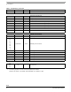
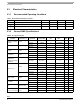
Table 5. Thermal Ratings
Symbol Description (Rating) Min. Max. Unit Notes
THERMAL RATINGS
T
A
Ambient Operating Temperature Range -40
85
°C
T
J
Operating Junction Temperature Range -40
125
°C
T
ST
Storage Temperature Range -65
150
°C
T
PPRT
Peak Package Reflow Temperature During Reflow -
Note 6
°C
(6),
(7)
THERMAL RESISTANCE AND PACKAGE DISSIPATION RATINGS
R
θJA
Junction to Ambient Natural Convection
• Single layer board (1s)
- 93 °C/W
(8),
(9)
R
θJMA
Junction to Ambient Natural Convection
• Four layer board (2s2p)
-
53 °C/W
(8),
(10)
R
θJMA
Junction to Ambient (@200 ft/min.)
• Single layer board (1s)
-
80 °C/W
(8),
(10)
R
θJMA
Junction to Ambient (@200 ft/min.)
• Four layer board (2s2p)
-
49 °C/W
(8),
(10)
R
θJB
Junction to Board
-
34 °C/W
(11)
R
θJC
Junction to Case
-
25 °C/W
(12)
THERMAL RESISTANCE AND PACKAGE DISSIPATION RATINGS (CONTINUED)
JT
Junction to Package Top
• Natural Convection
-
6.0 °C/W
(13)
Notes
6. Pin soldering temperature limit is for 10 seconds maximum duration. Not designed for immersion soldering. Exceeding these limits may
cause a malfunction or permanent damage to the device.
7. Freescale's Package Reflow capability meets the Pb-free requirements for JEDEC standard J-STD-020C, for Peak Package Reflow
Temperature and Moisture Sensitivity Levels (MSL).
8. Junction temperature is a function of on-chip power dissipation, package thermal resistance, mounting site (board) temperature, ambient
temperature, air flow, power dissipation of other components on the board, and board thermal resistance.
9. Per JEDEC JESD51-2 with the single layer board horizontal. Board meets JESD51-9 specification.
10. Per JEDEC JESD51-6 with the board horizontal.
11. Thermal resistance between the die and the printed circuit board per JEDEC JESD51-8. Board temperature is measured on the top
surface of the board near the package.
12. Thermal resistance between the die and the case top surface as measured by the cold plate method (MIL SPEC-883 Method 1012.1).
13. Thermal characterization parameter indicating the temperature difference between package top and the junction temperature per
JEDEC JESD51-2. When Greek letters are not available, the thermal characterization parameter is written as Psi-JT.