
Datasheet


Analog Integrated Circuit Device Data
27 Freescale Semiconductor
34709
Functional Block Description
7.3.2.2 Real Time Clock
A Real Time Clock (RTC) is provided with time and day counters as well as an alarm function. The RTC utilizes the 32.768 kHz
crystal oscillator for the time base and is powered by the coin cell backup supply when BP has dropped below operational range.
In configurations where the SRTC is used, the RTC can be disabled to conserve current drain by setting the RTCDIS bit to a 1
(defaults on at power up).
Time and Day Counters
The 32.768 kHz clock is divided into a 1.0 Hz time tick which drives a 17-bit Time Of Day (TOD) counter. The TOD counter counts
the seconds during a 24 hour period from 0 to 86,399 and will then roll over to 0. When the roll over occurs, it increments the
15-bit DAY counter. The DAY counter can count up to 32767 days. The 1.0 Hz time tick can be used to generate a 1HZI interrupt
if unmasked.
Time Of Day Alarm
A Time Of Day Alarm (TODA) function can be used to turn on the application and alert the processor. If the application is already
on, the processor will be interrupted. The TODA and DAYA registers are used to set the alarm time. When the TOD counter is
equal to the value in TODA and the DAY counter is equal to the value in DAYA, the TODAI interrupt will be generated.
Timer Reset
As long as the supply at BP is valid, the real time clock will be supplied from VCOREDIG. If BP is not valid, the real time clock
can be backed up from a coin cell via the LICELL pin. When the VSRTC voltage drops to the range of 0.9
V to 0.8 V, the
RTCPORB reset signal is generated and the contents of the RTC will be reset. Additional registers backed up by coin cell will
also reset with RTCPORB. To inform the processor that the contents of the RTC are no longer valid due to the reset, a timer reset
interrupt function is implemented with the RTCRSTI bit.
RTC Timer Calibration
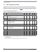
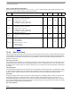
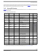
VSRTC - ACTIVE MODE - DC (CONTINUED)
V
SRTC
Output Voltage
•V
SRTCINMIN
< V
STRCIN
< V
SRTCINMAX
•I
SRTCMIN
< I
SRTC
< I
SRTCMAX
• PUMS[4:0] ≠ (0110, 0111, 1000, 1001)
• On, Standby, and Standby LPM modes
1.15 1.2 1.25 V
V
SRTC
Output Voltage
•V
SRTCINMIN
< V
STRCIN
< V
SRTCINMAX
•I
SRTCMIN
< I
SRTC
< I
SRTCMAX
• PUMS[4:0] = (0110, 0111, 1000, 1001)
• On, Standby, and Standby LPM modes
1.25 1.3 1.35 V
I
SRTCQ
Active Mode Quiescent Current
•V
SRTCINMIN
< V
STRCIN
< V
SRTCINMAX
•I
SRTC
= 0
- 0.8 - A
V
SRTCOS
Start-up Overshoot (IL = 0.0 mA)
• Battery insertion
• Coin cell insertion
Switchover Overshoot (IL = 0.0 mA)
• Battery to coin cell
• Coin cell to battery
- - 1.42 V
(35)
Notes
35. See workaround Figure 24.
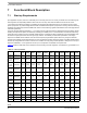
Table 15. VSRTC Electrical Specifications
Characteristics noted under conditions BP = 3.6 V, - 40 C T
A
85 C, unless otherwise noted. Typical values at BP = 3.6 V
and T
A
= 25 °C under nominal conditions, unless otherwise noted.
Symbol Characteristic Min Typ Max Unit Notes