
Datasheet

Analog Integrated Circuit Device Data
45 Freescale Semiconductor
34709
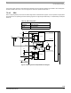
Functional Block Description
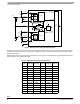
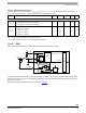
Figure 9. SW1 Dual Phase Output Mode Block Diagram
The peak current is sensed internally for over-current protection purposes. If an over-current condition is detected the regulator
will limit the current through cycle by cycle operation and alert the system through the SW1FAULT SPI bit and issue an SCPI
interrupt via the INT pin.
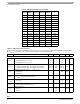
SW1A/B output voltage is SPI configurable in step sizes of 12.5 mV as shown in the table below. The SPI bits SW1A[5:0] set the
output voltage for both the SW1A and SW1B.
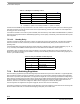
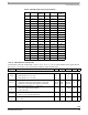
Table 35. SW1A/B Output Voltage Programmability
Set Point SW1A[5:0]
SW1A/B
Output (V)
Set Point SW1A[5:0]
SW1A/B
Output (V)
0 000000 0.6500 32 100000 1.0500
1 000001 0.6625 33 100001 1.0625
2 000010 0.6750 34 100010 1.0750
3 000011 0.6875 35 100011 1.0875
4 000100 0.7000 36 100100 1.1000
5 000101 0.7125 37 100101 1.1125
6 000110 0.7250 38 100110 1.1250
7 000111 0.7375 39 100111 1.1375
8 001000 0.7500 40 101000 1.1500
9 001001 0.7625 41 101001 1.1625
10 001010 0.7750 42 101010 1.1750
11 001011 0.7875 43 101011 1.1875
12 001100 0.8000 44 101100 1.2000
Driver
Controller
EA
Z1
Z2
Internal
Com pensation
SW1 IN
SW1ALX
SW1FB
I
SEN SE
C
OSW1A
C
IN SW 1A
L
SW 1A
SPI
Interface
GNDSW1A
SW1
SW1AMODE
SW1FAULT
V
REF
DAC
SPI
BP
Driver
Controller
SW1BIN
SW1BLX
I
SEN SE
C
OSW 1B
C
IN SW 1B
L
SW 1 B
GNDSW1B
SW1BMODE
BP
SW1CFG
D
SW1 A
D
SW 1B