
Datasheet


Analog Integrated Circuit Device Data
71 Freescale Semiconductor
34709
Functional Block Description
20% in series with the output capacitance is required. The total resistance includes the ESR of the capacitor plus an external
resistance provided by a discrete resistor or PCB circuit trace.
The nominal output voltage of this regulator can be configured through SPI and can be 2.5 V, 2.6 V, 2.7 V, or 2.775 V. The
maximum output current along the external PNP is 250
mA.
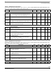
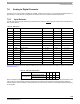
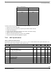
Table 60. VDAC Voltage Control
Parameter Value Output Voltage ILoad max
VDAC[1:0]
00 2.500 V 250 mA
01 2.600 V 250 mA
10 2.700 V 250 mA
11 2.775 V 250 mA
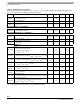
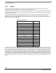
Table 61. VDAC Electrical Specification
Characteristics noted under conditions BP = 3.6 V, - 40 C T
A
85 C, unless otherwise noted. Typical values at BP = 3.6 V
and T
A
= 25 °C under nominal conditions, unless otherwise noted.
Symbol Characteristic Min Typ Max Unit Notes
GENERAL
V
DACIN
Operating Input Voltage Range V
INMIN
to V
INMAX
V
NOM
+
0.25
- 4.5 V
I
DAC
Operating Current Load Range IL
MIN
to IL
MAX
• Not exceeding PNP max power
0.0 - 250
mA
V
DACIN
Extended Input Voltage Range
• Performance may be out of specification
UVDET - 4.5
V
VDAC ACTIVE MODE – DC
V
DAC
Output Voltage V
OUT
V
NOM
– 3% V
NOM
V
NOM
+ 3% V
V
DACLOPP
Load Regulation
•1.0 mA < IL < IL
MAX
- 0.20 -
mV/mA
V
DACLIPP
Line Regulation
- 5.0 - mV
I
DACQ
Active Mode Quiescent Current
•IL = 0 mA
- 30 -
µA
I
DACDRVLIM
VDACDRV Base Current Limit
- 5.3 - mA
(58)
VDAC LOW-POWER MODE – DC - VDACMODE=1
V
DAC
Output Voltage V
OUT
V
NOM
– 3% V
NOM
V
NOM
+ 3% V
I
DAC
Current Load Range IL
MINLP
to IL
MAXLP
0.0 - 3.0 mA
I
DACQ
Low-power Mode Quiescent Current
•IL = 0 mA
- 8.0 -
µA
VDAC ACTIVE MODE – AC
VDAC
PSRR
PSRR
IL = 75% of IL
MAX
20 Hz to 20 kHz
•V
DACIN
= V
INMIN
+ 100 mV
•V
DACIN
= V
NOM
+ 1.0 V
-
-
50
50
-
-
dB
t
ON-VDAC
Turn-on Time
• Enable to 90% of end value V
DACIN
= V
INMIN
, V
INMAX
; IL = 0 mA
- - 1.0
ms