
Datasheet

Analog Integrated Circuit Device Data
81 Freescale Semiconductor
34709
Functional Block Description
7.7 Auxiliary Circuits
7.7.1 General Purpose I/Os
The 34709 contains four configurable GPIO input/outputs for general purpose use. When configured as outputs, they can be
configured as open-drain (OD) or CMOS (push-pull outputs). These GPIOs are low-voltage capable (1.2 or 1.8
V). In open-drain
configuration these outputs can only be pulled up to 2.5
V maximum.
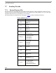
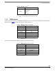
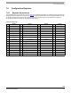
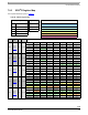
Each individual GPIO has a dedicated 16-bit control register. Table 74 provides the detailed bit descriptions.
Table 74. GPIOLVx Control
(60)
SPI Bit Description
DIR
GPIOLVx direction
0: Input (default)
1: Output
DIN
Input state of the GPIOLVx pin
0: Input low
1: Input High
DOUT
Output state of GPIOLVx pin
0: Output Low
1: Output High
HYS
Hysteresis
0: CMOS in
1: Hysteresis (default)
DBNC[1:0]
GPIOLVx input debounce time
00: no debounce (default)
01: 10 ms debounce
10: 20 ms debounce
11: 30 mS debounce
INT[1:0]
GPIOLVx interrupt control
00: None (default)
01: Falling edge
10: Rising edge
11: Both edges
PKE
Pad keep enable
0: Off (default)
1: On
ODE
Open-drain enable
0: CMOS (default)
1: OD
DSE
Drive strength enable
0: 4.0 mA (default)
1: 8.0 mA
PUE
Pull-up/down enable
0: pull-up/down off
1: pull-up/down on (default)
PUS[1:0]
Pull-up/Pull-down enable
00: 10 K active pull-down
01: 10 K active pull-up
10: 100 K active pull-down
11: 100 K active pull-up (default)