
Datasheet

Analog Integrated Circuit Device Data
Freescale Semiconductor 82
34709
Functional Block Description
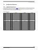
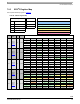
7.7.2 PWM Outputs
There are two PWM outputs on the 34709 PWM1 and PWM2 and which are controlled by the PWMxDUTY and PWMxCLKDIV
registers shown in
Table 75.The base clock will be the 2.0 MHz divided by 32.
32.768 kHz Crystal Oscillator RTC Block Description and Application Information
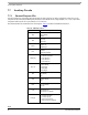
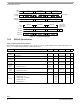
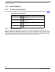
SRE[1:0]
Slew rate enable
00: slow (default)
01: normal
10: fast
11: very fast
Notes
60. x= 0, 1, 2, or 3 depending of the GPIO channel it is being
used
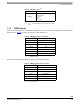
Table 75. PWMx Duty Cycle Programming
PWMxDC[5:0](
(61)
) Duty Cycle
000000 0/32, Off (default)
000001 1/32
… …
010000 16/32
… …
011111 31/32
1xxxxx 32/32, Continuously On
Notes
61. “x” represent 1 and 2
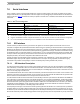
Table 76. PWMx Clock Divider Programming
PWMxCLKDIV[5:0](
(62)
) Duty Cycle
000000 Base Clock
000001 Base Clock / 2
… …
001111 Base Clock / 16
… …
111111 Base Clock / 64
Notes
62. “x” represent 1 and 2
Table 74. GPIOLVx Control
(60)
SPI Bit Description