56F8365/56F8165 Data Sheet Technical Data 56F8300 16-bit Digital Signal Controllers MC56F8365 Rev. 9 02/2012 freescale.
Document Revision History Version History Description of Change Rev 0 Pre-release, Alpha customers only Rev 1.0 Initial Public Release Rev 2.0 Added output voltage maximum value and note to clarify in Table 10-1; also removed overall life expectancy note, since life expectancy is dependent on customer usage and must be determined by reliability engineering. Clarified value and unit measure for Maximum allowed PD in Table 10-3. Corrected note about average value for Flash Data Retention in Table 10-4.
Table of Contents Part 1: Overview 5 1.1. 1.2. 1.3. 1.4. 1.5. 1.6. 56F8365/56F8165 Features 5 Device Description 8 Award-Winning Development Environment 10 Architecture Block Diagram 10 Product Documentation 13 Data Sheet Conventions 14 Part 2: Signal/Connection Descriptions 14 Part 3: On-Chip Clock Synthesis (OCCS) 36 3.1. Introduction 36 3.2. External Clock Operation 36 3.3.
56F8365/56F8165 General Description Note: Features in italics are NOT available in the 56F8165 device.
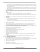
6F8365/56F8165 Features RSTO 5 RESET 6 PWM Outputs 3 Current Sense Inputs or GPIOD 4 Fault Inputs 4 AD0 4 AD0 ADCB AD1 Temp_Sense 2 Analog Reg Low Voltage Supervisor Data ALU 16 x 16 + 36 -> 36-Bit MAC Three 16-bit Input Registers Four 36-bit Accumulators Bit Manipulation Unit R/W Control Memory 4 4 VSSA ADCA VREF 4 VDDA 2 PAB PDB CDBR CDBW AD1 5 4 5 Digital Reg Address Generation Unit Program Controller and Hardware Looping Unit PWMB 7 16-Bit 56800E Core Fault Inputs 6
• • • • • • 1.1.2 Four internal data buses Instruction set supports both DSP and controller functions Controller-style addressing modes and instructions for compact code Efficient C compiler and local variable support Software subroutine and interrupt stack with depth limited only by memory JTAG/EOnCE debug programming interface Differences Between Devices Table 1-1 outlines the key differences between the 56F8365 and 56F8165 devices. Table 1-1 Device Differences 1.1.
56F8365/56F8165 Features — In the 56F8365, two Pulse Width Modulator modules, each with six PWM outputs, three Current Sense inputs, and four Fault inputs; fault-tolerant design with dead time insertion; supports both center-aligned and edge-aligned modes — In the 56F8165, one Pulse Width Modulator module with six PWM outputs, three Current Sense inputs and three Fault inputs; fault-tolerant design with dead time insertion; supports both center-aligned and edge-aligned modes • • Four 12-bit, Analog-to-Dig
1.2 Device Description The 56F8365 and 56F8165 are members of the 56800E core-based family of controllers. Each combines, on a single chip, the processing power of a Digital Signal Processor (DSP) and the functionality of a microcontroller with a flexible set of peripherals to create an extremely cost-effective solution. Because of their low cost, configuration flexibility, and compact program code, the 56F8365 and 56F8165 are well-suited for many applications.
Device Description The 56F8365 incorporates two Quadrature Decoders capable of capturing all four transitions on the two-phase inputs, permitting generation of a number proportional to actual position. Speed computation capabilities accommodate both fast- and slow-moving shafts. An integrated watchdog timer in the Quadrature Decoder can be programmed with a time-out value to alert when no shaft motion is detected. Each input is filtered to ensure only true transitions are recorded.
internal interrupt controller is also a part of the 56F8165. 1.3 Award-Winning Development Environment Processor ExpertTM (PE) provides a Rapid Application Design (RAD) tool that combines easy-to-use component-based software application creation with an expert knowledge system. The CodeWarrior Integrated Development Environment is a sophisticated tool for code navigation, compiling, and debugging. A complete set of evaluation modules (EVMs) and development system cards will support concurrent engineering.
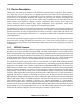
Architecture Block Diagram 5 JTAG / EOnCE Boot Flash pdb_m[15:0] pab[20:0] Program Flash cdbw[31:0] Program RAM 56800E EMI* CHIP TAP Controller TAP Linking Module 11 4 6 xab1[23:0] Address Data Control Data RAM xab2[23:0] External JTAG Port Data Flash cdbr_m[31:0] xdb2_m[15:0] IPBus Bridge Flash Memory Module NOT available on the 56F8165 device.
To/From IPBus Bridge Interrupt Controller CLKGEN (OSC/PLL) Low Voltage Interrupt Timer A 4 POR and LVI System POR Quadrature Decoder 0 RESET SIM 4 Timer D COP Reset COP Timer B 4 2 FlexCAN Quadrature Decoder 1 2 FlexCAN2 SPI1 13 PWMA GPIOA SYNC Output 13 PWMB GPIOB SYNC Output GPIOC ch2i ch3i GPIOD Timer C ch3i GPIOE 2 ch2i GPIOF 4 ADCB 8 SPI0 2 SCI0 2 SCI1 8 ADCA TEMP_SENSE IPBus NOT available on the 56F8165 device.
Product Documentation Figure 1-2 Peripheral Subsystem Table 1-2 Bus Signal Names Name Function Program Memory Interface pdb_m[15:0] Program data bus for instruction word fetches or read operations. cdbw[15:0] Primary core data bus used for program memory writes. (Only these 16 bits of the cdbw[31:0] bus are used for writes to program memory.) pab[20:0] Program memory address bus. Data is returned on pdb_m bus. Primary Data Memory Interface Bus cdbr_m[31:0] Primary core data bus for memory reads.
Table 1-3 Chip Documentation Topic Description Order Number 56F8300 SCI/CAN Bootloader User Manual Detailed description of the SCI/CAN Bootloaders 56F8300 family of devices MC56F83xxBLUM 56F8365/56F8165 Technical Data Sheet Electrical and timing specifications, pin descriptions, device specific peripheral information and package descriptions (this document) MC56F8365 Errata Details any chip issues that might be present MC56F8365E MC56F8165E 1.
Introduction Table 2-1 Functional Group Pin Allocations Number of Pins in Package Functional Group 56F8365 56F8165 Power (VDD or VDDA) 9 9 Power Option Control 1 1 Ground (VSS or VSSA) 6 6 Supply Capacitors1 & VPP 6 6 PLL and Clock 4 4 Bus Control 6 6 Interrupt and Program Control 4 4 Pulse Width Modulator (PWM) Ports 26 13 Serial Peripheral Interface (SPI) Port 0 4 4 Serial Peripheral Interface (SPI) Port 1 — 4 Quadrature Decoder Port 02 4 4 Quadrature Decoder Port 13 4
Power VDD_IO Power VDDA_OSC_PLL Power VDDA_ADC Ground VSS Ground VSSA_ADC OCR_DIS Other Supply Ports VCAP1 - VCAP4 VPP1 & VPP2 CLKMODE PLL and Clock *External Address Bus or GPIO *External Data Bus EXTAL XTAL CLKO A8 - A13 (GPIOA0 - 5) GPIOB0-4 (A16 - 20) D7 - D10 (GPIOF0 - 3) 7 1 1 1 1 1 5 1 1 1 4 2 1 1 1 56F8365 1 1 1 1 1 1 1 1 Bus Control GPIOD0 (CS2, CAN2_TX) GPIOD1 (CS3, CAN2_RX) GPIOD2 - 5 (CS4 - 7) 6 6 3 4 SCI1 or GPIO JTAG/ EOnCE Port TXD0 (GPIOE0) RXD0 (GPIOE1) TXD1 (
Introduction Power VDD_IO Power VDDA_ADC Power VDDA_OSC_PLL Ground VSS Ground VSSA_ADC OCR_DIS VCAP1 - VCAP4 Other Supply Ports VPP1 & VPP2 CLKMODE PLL and Clock EXTAL XTAL CLKO 7 1 1 1 1 5 1 1 1 56F8165 1 1 1 4 2 1 1 1 1 1 1 1 1 1 1 *External A8 - A13 (GPIOA0 - 5) Address Bus or GPIO GPIOB0-4 (A16 - 20) *External D7 - D10 (GPIOF0 - 3) Data Bus Bus Control GPIOD0 - 5 (CS2 - 7) 5 3 6 4 3 8 6 5 8 TXD0 (GPIOE0) SCI0 or GPIOE RXD0 (GPIOE1) SCI1 or GPIO TXD1 (GPIOD6
2.2 Signal Pins After reset, each pin is configured for its primary function (listed first). Any alternate functionality must be programmed. EMI is not functional in this package; since only part of the address/data bus is bonded out, use as GPIO pins. Note: Signals in italics are NOT available in the 56F8165 device. If the “State During Reset” lists more than one state for a pin, the first state is the actual reset state.
Signal Pins Table 2-2 Signal and Package Information for the 128-Pin LQFP (Continued) State During Reset Signal Name Pin No. Type VSS 3 Supply Ground — These pins provide ground for chip logic and I/O drivers. VSS 21 VSS 35 VSS 59 VSS 65 VSSA_ADC 95 Supply ADC Analog Ground — This pin supplies an analog ground to the ADC modules.
Table 2-2 Signal and Package Information for the 128-Pin LQFP (Continued) Signal Name Pin No. Type XTAL 73 Input/ Output State During Reset Chip-driven Signal Description Crystal Oscillator Output — This output connects the internal crystal oscillator output to an external crystal. If an external clock is used, XTAL must be used as the input and EXTAL connected to GND. The input clock can be selected to provide the clock directly to the core.
Signal Pins Table 2-2 Signal and Package Information for the 128-Pin LQFP (Continued) Signal Name Pin No. Type State During Reset GPIOB0 27 Schmitt Input/ Output Input, pull-up enabled (A16) GPIOB1 Output 28 29 After reset, the default state is GPIO. (A18) GPIOB3 To deactivate the internal pull-up resistor, clear bit 0 in the GPIOB_PUR register. 30 Example: GPIOB1, clear bit 1 in the GPIOB_PUR register.
Table 2-2 Signal and Package Information for the 128-Pin LQFP (Continued) Signal Name Pin No. Type D7 22 Input/ Output (GPIOF0) D8 (GPIOF1) 23 D9 (GPIOF2) 24 D10 (GPIOF3) 26 State During Reset In reset, output is disabled, pull-up is enabled Input/ Output Signal Description Data Bus — D7 - D10 specify part of the data for external program or data memory accesses.
Signal Pins Table 2-2 Signal and Package Information for the 128-Pin LQFP (Continued) Signal Name Pin No. Type State During Reset GPIOD1 43 Schmitt Input/ Output Input, pull-up enabled Output (CS3) Signal Description Port D GPIO — This GPIO pin can be individually programmed as an input or output pin. Chip Select — CS3 may be programmed within the EMI module to act as a chip select for specific areas of the external memory map.
Table 2-2 Signal and Package Information for the 128-Pin LQFP (Continued) Signal Name Pin No. Type TXD0 7 Output (GPIOE0) Input/ Output State During Reset In reset, output is disabled, pull-up is enabled Signal Description Transmit Data — SCI0 transmit data output Port E GPIO — This GPIO pin can be individually programmed as an input or output pin. After reset, the default state is SCI output. To deactivate the internal pull-up resistor, clear bit 0 in the GPIOE_PUR register.
Signal Pins Table 2-2 Signal and Package Information for the 128-Pin LQFP (Continued) Signal Name Pin No. Type TMS 116 Schmitt Input State During Reset Signal Description Input, pulled high internally Test Mode Select Input — This input pin is used to sequence the JTAG TAP controller’s state machine. It is sampled on the rising edge of TCK and has an on-chip pull-up resistor. To deactivate the internal pull-up resistor, set the JTAG bit in the SIM_PUDR register.
Table 2-2 Signal and Package Information for the 128-Pin LQFP (Continued) Signal Name Pin No. Type PHASEA0 127 Schmitt Input State During Reset Input, pull-up enabled Signal Description Phase A — Quadrature Decoder 0, PHASEA input (TA0) Schmitt Input/ Output TA0 — Timer A, Channel 0 (GPIOC4) Schmitt Input/ Output Port C GPIO — This GPIO pin can be individually programmed as an input or output pin. After reset, the default state is PHASEA0.
Signal Pins Table 2-2 Signal and Package Information for the 128-Pin LQFP (Continued) Signal Name Pin No. Type HOME0 2 Schmitt Input State During Reset Input, pull-up enabled Signal Description Home — Quadrature Decoder 0, HOME input (TA3) Schmitt Input/ Output TA3 — Timer A, Channel 3 (GPIOC7) Schmitt Input/ Output Port C GPIO — This GPIO pin can be individually programmed as an input or output pin. After reset, the default state is HOME0.
Table 2-2 Signal and Package Information for the 128-Pin LQFP (Continued) Signal Name Pin No. Type MISO0 125 Input/ Output (GPIOE6) State During Reset Input, pull-up enabled Input/ Output Signal Description SPI 0 Master In/Slave Out — This serial data pin is an input to a master device and an output from a slave device. The MISO line of a slave device is placed in the high-impedance state if the slave device is not selected.
Signal Pins Table 2-2 Signal and Package Information for the 128-Pin LQFP (Continued) Signal Name Pin No. Type PHASEB1 10 Schmitt Input State During Reset Input, pull-up enabled Signal Description Phase B1 — Quadrature Decoder 1, PHASEB input for decoder 1. (TB1) Schmitt Input/ Output TB1 — Timer B, Channel 1 (MOSI1) Schmitt Input/ Output SPI 1 Master Out/Slave In — This serial data pin is an output from a master device and an input to a slave device.
Table 2-2 Signal and Package Information for the 128-Pin LQFP (Continued) Signal Name Pin No. Type INDEX1 11 Schmitt Input State During Reset Input, pull-up enabled Signal Description Index1 — Quadrature Decoder 1, INDEX input (TB2) Schmitt Input/ Output TB2 — Timer B, Channel 2 (MISO1) Schmitt Input/ Output SPI 1 Master In/Slave Out — This serial data pin is an input to a master device and output from a slave device.
Signal Pins Table 2-2 Signal and Package Information for the 128-Pin LQFP (Continued) State During Reset Signal Name Pin No. Type PWMA0 58 Output PWMA0 - 5 — These are six PWMA output pins. PWMA1 60 In reset, output is disabled PWMA2 61 PWMA3 63 PWMA4 64 PWMA5 66 ISA0 104 Schmitt Input Input, pull-up enabled ISA0 - 2 — These three input current status pins are used for top/bottom pulse width correction in complementary channel operation for PWMA.
Table 2-2 Signal and Package Information for the 128-Pin LQFP (Continued) State During Reset Signal Name Pin No. Type PWMB0 32 Output PWMB0 - 5 — Six PWMB output pins. PWMB1 33 In reset, output is disabled PWMB2 34 PWMB3 37 PWMB4 38 PWMB5 39 ISB0 48 Schmitt Input Input, pull-up enabled ISB0 - 2 — These three input current status pins are used for top/bottom pulse width correction in complementary channel operation for PWMB.
Signal Pins Table 2-2 Signal and Package Information for the 128-Pin LQFP (Continued) State During Reset Signal Description Input/ Output Analog Input/ Output VREFP, VREFMID & VREFN — Internal pins for voltage reference which are brought off-chip so that they can be bypassed. Connect to a 0.1 F low ESR capacitor. 89 Input Analog Input VREFLO — Analog Reference Voltage Low. This should normally be connected to a low-noise VSSA.
Table 2-2 Signal and Package Information for the 128-Pin LQFP (Continued) Signal Name Pin No. Type State During Reset TC0 111 Schmitt Input/ Output Input, pull-up enabled (GPIOE8) TC1 (GPIOE9) 113 Schmitt Input/ Output Signal Description TC0 - 1 — Timer C, Channels 0 and 1 Port E GPIO — These GPIO pins can be individually programmed as input or output pins. At reset, these pins default to Timer functionality.
Signal Pins Table 2-2 Signal and Package Information for the 128-Pin LQFP (Continued) Signal Name Pin No. Type RESET 78 Schmitt Input State During Reset Input, pull-up enabled Signal Description Reset — This input is a direct hardware reset on the processor. When RESET is asserted low, the device is initialized and placed in the reset state. A Schmitt trigger input is used for noise immunity.
Part 3 On-Chip Clock Synthesis (OCCS) 3.1 Introduction Refer to the OCCS chapter of the 56F8300 Peripheral User Manual for a full description of the OCCS. The material contained here identifies the specific features of the OCCS design. Figure 3-1 shows the specific OCCS block diagram to reference in the OCCS chapter of the 56F8300 Peripheral User Manual.
External Clock Operation The crystal and associated components should be mounted as near as possible to the EXTAL and XTAL pins to minimize output distortion and start-up stabilization time.
3.2.3 External Clock Source The recommended method of connecting an external clock is illustrated in Figure 3-4. The external clock source is connected to XTAL and the EXTAL pin is grounded. Set OCCS_COHL bit high when using an external clock source as well. XTAL EXTAL External Clock VSS Note: When using an external clocking source with this configuration, the input “CLKMODE” should be high and the COHL bit in the OSCTL register should be set to 1.
Program Map Table 4-1 Chip Memory Configurations On-Chip Memory 56F8365 56F8165 Use Restrictions Data Flash 32KB — Erase/Program via Flash interface unit and word writes to CDBW. Data Flash can be read via either CDBR or XDB2, but not by both simultaneously Program RAM 4KB — None Data RAM 32KB 32KB None Program Boot Flash 32KB 32KB Erase/Program via Flash Interface unit and word writes to CDBW 4.2 Program Map The Program memory map is located in Table 4-4.
Table 4-3 Changing OMR MA Value During Normal Operation OMR MA Chip Operating Mode 0 Use internal P-space memory map configuration 11 Use external P-space memory map configuration – If MB = 0 at reset, changing this bit has no effect. 1. Setting this bit can cause unpredictable results and is not recommended, since the EMI is not functional in this package. Table 4-4 shows the memory map options of the 56F8365/56F8165.
Interrupt Vector Table 5. Not accessible in reset configuration, since the address is above P:$00 FFFF. The higher bit address/GPIO (and/or chip selects) pins must be reconfigured before this external memory is accessible. 6. Not accessible in this part, since the EMI is not fully pinned out in this package; information in shaded areas not applicable to 56F8365/56F8165. 7. Two independent program flash blocks allow one to be programmed/erased while executing from another.
Table 4-5 Interrupt Vector Table Contents1 (Continued) Peripheral Vector Number Priority Level Vector Base Address + Interrupt Function core 14 2 P:$1C SW Interrupt 2 core 15 1 P:$1E SW Interrupt 1 core 16 0 P:$20 SW Interrupt 0 core 17 0-2 P:$22 IRQA core 18 0-2 P:$24 IRQB Reserved LVI 20 0-2 P:$28 Low-Voltage Detector (power sense) PLL 21 0-2 P:$2A PLL FM 22 0-2 P:$2C FM Access Error Interrupt FM 23 0-2 P:$2E FM Command Complete FM 24 0-2 P:$30 FM Comm
Interrupt Vector Table Table 4-5 Interrupt Vector Table Contents1 (Continued) Peripheral Vector Number Priority Level Vector Base Address + Interrupt Function DEC1 47 0-2 P:$5E Quadrature Decoder #1 Home Switch or Watchdog DEC1 48 0-2 P:$60 Quadrature Decoder #1 INDEX Pulse DEC0 49 0-2 P:$62 Quadrature Decoder #0 Home Switch or Watchdog DEC0 50 0-2 P:$64 Quadrature Decoder #0 INDEX Pulse Reserved TMRD 52 0-2 P:$68 Timer D, Channel 0 TMRD 53 0-2 P:$6A Timer D, Channel 1 TM
Table 4-5 Interrupt Vector Table Contents1 (Continued) Peripheral Vector Number Priority Level Vector Base Address + Interrupt Function PWMB 79 0-2 P:$9E PWM B Fault PWMA 80 0-2 P:$A0 PWM A Fault core 81 -1 P:$A2 SW Interrupt LP FLEXCAN2 82 0-2 P:$A4 FlexCAN Bus-Off FLEXCAN2 83 0-2 P:$A6 FlexCAN Error FLEXCAN2 84 0-2 P:$A8 FlexCAN Wake Up FLEXCAN2 85 0-2 P:$AA FlexCAN Message Buffer Interrupt 1. Two words are allocated for each entry in the vector table.
Flash Memory Map 4.5 Flash Memory Map Figure 4-1 illustrates the Flash Memory (FM) map on the system bus. The Flash Memory is divided into three functional blocks. The Program and boot memories reside on the Program Memory buses. They are controlled by one set of banked registers. Data Memory Flash resides on the Data Memory buses and is controlled separately by its own set of banked registers. The top nine words of the Program Memory Flash are treated as special memory locations.
Table 4-7. Flash Memory Partitions Flash Size Sectors Sector Size Page Size Program Flash 512KB 16 16K x 16 bits 1024x 16 bits Data Flash 32KB 16 1024 x 16 bits 256 x 16 bits Boot Flash 32KB 4 4K x 16 bits 512 x 16 bits Please see the 56F8300 Peripheral User Manual for additional Flash information. 4.
Peripheral Memory Mapped Registers Table 4-8 EOnCE Memory Map (Continued) Address Register Acronym Register Name X:$FF FF9F — Instruction Step Counter X:$FF FFA0 OCR (bits) Control Register Reserved X:$FF FFFC OCLSR (8 bits) Core Lock / Unlock Status Register X:$FF FFFD OTXRXSR (8 bits) Transmit and Receive Status and Control Register X:$FF FFFE OTX / ORX (32 bits) Transmit Register / Receive Register X:$FF FFFF OTX1 / ORX1 Transmit Register Upper Word Receive Register Upper Word 4.
Table 4-9 Data Memory Peripheral Base Address Map Summary (Continued) Peripheral Prefix Base Address Table Number Temperature Sensor TSENSOR X:$00 F270 4-22 SCI #0 SCI0 X:$00 F280 4-23 SCI #1 SCI1 X:$00 F290 4-24 SPI #0 SPI0 X:$00 F2A0 4-25 SPI #1 SPI1 X:$00 F2B0 4-26 COP COP X:$00 F2C0 4-27 PLL, OSC CLKGEN X:$00 F2D0 4-28 GPIO Port A GPIOA X:$00 F2E0 4-29 GPIO Port B GPIOB X:$00 F300 4-30 GPIO Port C GPIOC X:$00 F310 4-31 GPIO Port D GPIOD X:$00 F320 4-32 GPI
Peripheral Memory Mapped Registers Table 4-10 External Memory Integration Registers Address Map (EMI_BASE = $00 F020) Address Offset Register Description CSBAR 0 $0 Chip Select Base Address Register 0 CSBAR 1 $1 Chip Select Base Address Register 1 CSBAR 2 $2 Chip Select Base Address Register 2 CSBAR 3 $3 Chip Select Base Address Register 3 CSBAR 4 $4 Chip Select Base Address Register 4 CSBAR 5 $5 Chip Select Base Address Register 5 CSBAR 6 $6 Chip Select Base Address Register 6 CSBAR
Table 4-11 Quad Timer A Registers Address Map (Continued) (TMRA_BASE = $00 F040) Register Acronym Address Offset Register Description TMRA0_CMP2 $1 Compare Register 2 TMRA0_CAP $2 Capture Register TMRA0_LOAD $3 Load Register TMRA0_HOLD $4 Hold Register TMRA0_CNTR $5 Counter Register TMRA0_CTRL $6 Control Register TMRA0_SCR $7 Status and Control Register TMRA0_CMPLD1 $8 Comparator Load Register 1 TMRA0_CMPLD2 $9 Comparator Load Register 2 TMRA0_COMSCR $A Comparator Status and
Peripheral Memory Mapped Registers Table 4-11 Quad Timer A Registers Address Map (Continued) (TMRA_BASE = $00 F040) Register Acronym Address Offset Register Description TMRA2_CMPLD2 $29 Comparator Load Register 2 TMRA2_COMSCR $2A Comparator Status and Control Register Reserved TMRA3_CMP1 $30 Compare Register 1 TMRA3_CMP2 $31 Compare Register 2 TMRA3_CAP $32 Capture Register TMRA3_LOAD $33 Load Register TMRA3_HOLD $34 Hold Register TMRA3_CNTR $35 Counter Register TMRA3_CTRL $36
Table 4-12 Quad Timer B Registers Address Map (Continued) (TMRB_BASE = $00 F080) Quad Timer B is NOT available in the 56F8165 device Register Acronym Address Offset Register Description TMRB1_CMP2 $11 Compare Register 2 TMRB1_CAP $12 Capture Register TMRB1_LOAD $13 Load Register TMRB1_HOLD $14 Hold Register TMRB1_CNTR $15 Counter Register TMRB1_CTRL $16 Control Register TMRB1_SCR $17 Status and Control Register TMRB1_CMPLD1 $18 Comparator Load Register 1 TMRB1_CMPLD2 $19 Compara
Peripheral Memory Mapped Registers Table 4-12 Quad Timer B Registers Address Map (Continued) (TMRB_BASE = $00 F080) Quad Timer B is NOT available in the 56F8165 device Register Acronym Address Offset Register Description TMRB3_CMPLD1 $38 Comparator Load Register 1 TMRB3_CMPLD2 $39 Comparator Load Register 2 TMRB3_COMSCR $3A Comparator Status and Control Register Table 4-13 Quad Timer C Registers Address Map (TMRC_BASE = $00 F0C0) Register Acronym Address Offset Register Description TMRC0_CMP
Table 4-13 Quad Timer C Registers Address Map (Continued) (TMRC_BASE = $00 F0C0) Register Acronym Address Offset Register Description TMRC2_CMP1 $20 Compare Register 1 TMRC2_CMP2 $21 Compare Register 2 TMRC2_CAP $22 Capture Register TMRC2_LOAD $23 Load Register TMRC2_HOLD $24 Hold Register TMRC2_CNTR $25 Counter Register TMRC2_CTRL $26 Control Register TMRC2_SCR $27 Status and Control Register TMRC2_CMPLD1 $28 Comparator Load Register 1 TMRC2_CMPLD2 $29 Comparator Load Regist
Peripheral Memory Mapped Registers Table 4-14 Quad Timer D Registers Address Map (Continued) (TMRD_BASE = $00 F100) Quad Timer D is NOT available in the 56F8165 device Register Acronym Address Offset Register Description TMRD0_HOLD $4 Hold Register TMRD0_CNTR $5 Counter Register TMRD0_CTRL $6 Control Register TMRD0_SCR $7 Status and Control Register TMRD0_CMPLD1 $8 Comparator Load Register 1 TMRD0_CMPLD2 $9 Comparator Load Register 2 TMRD0_COMSCR $A Comparator Status and Control Regi
Table 4-14 Quad Timer D Registers Address Map (Continued) (TMRD_BASE = $00 F100) Quad Timer D is NOT available in the 56F8165 device Register Acronym Address Offset Register Description Reserved TMRD3_CMP1 $30 Compare Register 1 TMRD3_CMP2 $31 Compare Register 2 TMRD3_CAP $32 Capture Register TMRD3_LOAD $33 Load Register TMRD3_HOLD $34 Hold Register TMRD3_CNTR $35 Counter Register TMRD3_CTRL $36 Control Register TMRD3_SCR $37 Status and Control Register TMRD3_CMPLD1 $38 Comparat
Peripheral Memory Mapped Registers Table 4-15 Pulse Width Modulator A Registers Address Map (Continued) (PWMA_BASE = $00 F140) PWMA is NOT available in the 56F8165 device Register Acronym Address Offset Register Description PWMA_PMDISMAP2 $E Disable Mapping Register 2 PWMA_PMCFG $F Configure Register PWMA_PMCCR $10 Channel Control Register PWMA_PMPORT $11 Port Register PWMA_PMICCR $12 PWM Internal Correction Control Register Table 4-16 Pulse Width Modulator B Registers Address Map (PWMB_B
Table 4-17 Quadrature Decoder 0 Registers Address Map (DEC0_BASE = $00 F180) Register Acronym Address Offset Register Description DEC0_DECCR $0 Decoder Control Register DEC0_FIR $1 Filter Interval Register DEC0_WTR $2 Watchdog Time-out Register DEC0_POSD $3 Position Difference Counter Register DEC0_POSDH $4 Position Difference Counter Hold Register DEC0_REV $5 Revolution Counter Register DEC0_REVH $6 Revolution Hold Register DEC0_UPOS $7 Upper Position Counter Register DEC0_LPOS
Peripheral Memory Mapped Registers Table 4-18 Quadrature Decoder 1 Registers Address Map (Continued) (DEC1_BASE = $00 F190) Quadrature Decoder 1 is NOT available in the 56F8165 device Register Acronym DEC1_IMR Address Offset $D Register Description Input Monitor Register Table 4-19 Interrupt Control Registers Address Map (ITCN_BASE = $00 F1A0) Register Acronym Address Offset Register Description IPR 0 $0 Interrupt Priority Register 0 IPR 1 $1 Interrupt Priority Register 1 IPR 2 $2 Interrupt P
Table 4-19 Interrupt Control Registers Address Map (Continued) (ITCN_BASE = $00 F1A0) Register Acronym IPR10 Address Offset $1F Register Description Interrupt Priority Register 10 Table 4-20 Analog-to-Digital Converter Registers Address Map (ADCA_BASE = $00 F200) Register Acronym Address Offset Register Description ADCA_CR1 $0 Control Register 1 ADCA_CR2 $1 Control Register 2 ADCA_ZCC $2 Zero Crossing Control Register ADCA_LST 1 $3 Channel List Register 1 ADCA_LST 2 $4 Channel List Regis
Peripheral Memory Mapped Registers Table 4-20 Analog-to-Digital Converter Registers Address Map (Continued) (ADCA_BASE = $00 F200) Register Acronym Address Offset Register Description ADCA_HLMT 2 $1B High Limit Register 2 ADCA_HLMT 3 $1C High Limit Register 3 ADCA_HLMT 4 $1D High Limit Register 4 ADCA_HLMT 5 $1E High Limit Register 5 ADCA_HLMT 6 $1F High Limit Register 6 ADCA_HLMT 7 $20 High Limit Register 7 ADCA_OFS 0 $21 Offset Register 0 ADCA_OFS 1 $22 Offset Register 1 ADCA_O
Table 4-21 Analog-to-Digital Converter Registers Address Map (Continued) (ADCB_BASE = $00 F240) Register Acronym Address Offset Register Description ADCB_RSLT 3 $C Result Register 3 ADCB_RSLT 4 $D Result Register 4 ADCB_RSLT 5 $E Result Register 5 ADCB_RSLT 6 $F Result Register 6 ADCB_RSLT 7 $10 Result Register 7 ADCB_LLMT 0 $11 Low Limit Register 0 ADCB_LLMT 1 $12 Low Limit Register 1 ADCB_LLMT 2 $13 Low Limit Register 2 ADCB_LLMT 3 $14 Low Limit Register 3 ADCB_LLMT 4 $15 L
Peripheral Memory Mapped Registers Table 4-22 Temperature Sensor Register Address Map (TSENSOR_BASE = $00 F270) Temperature Sensor is NOT available in the 56F8165 device Register Acronym TSENSOR_CNTL Address Offset $0 Register Description Control Register Table 4-23 Serial Communication Interface 0 Registers Address Map (SCI0_BASE = $00 F280) Register Acronym Address Offset Register Description SCI0_SCIBR $0 Baud Rate Register SCI0_SCICR $1 Control Register Reserved SCI0_SCISR $3 Status Regis
Table 4-26 Serial Peripheral Interface 1 Registers Address Map (SPI1_BASE = $00 F2B0) Register Acronym Address Offset Register Description SPI1_SPSCR $0 Status and Control Register SPI1_SPDSR $1 Data Size Register SPI1_SPDRR $2 Data Receive Register SPI1_SPDTR $3 Data Transmitter Register Table 4-27 Computer Operating Properly Registers Address Map (COP_BASE = $00 F2C0) Register Acronym Address Offset Register Description COPCTL $0 Control Register COPTO $1 Time Out Register COPCTR
Peripheral Memory Mapped Registers Table 4-29 GPIOA Registers Address Map (Continued) (GPIOA_BASE = $00 F2E0) Register Acronym Address Offset Register Description Reset Value GPIOA_IAR $4 Interrupt Assert Register 0 x 0000 GPIOA_IENR $5 Interrupt Enable Register 0 x 0000 GPIOA_IPOLR $6 Interrupt Polarity Register 0 x 0000 GPIOA_IPR $7 Interrupt Pending Register 0 x 0000 GPIOA_IESR $8 Interrupt Edge-Sensitive Register 0 x 0000 GPIOA_PPMODE $9 Push-Pull Mode Register 0 x 3FFF GPIO
Table 4-31 GPIOC Registers Address Map (Continued) (GPIOC_BASE = $00 F310) Register Acronym Address Offset Register Description Reset Value GPIOC_IENR $5 Interrupt Enable Register 0 x 0000 GPIOC_IPOLR $6 Interrupt Polarity Register 0 x 0000 GPIOC_IPR $7 Interrupt Pending Register 0 x 0000 GPIOC_IESR $8 Interrupt Edge-Sensitive Register 0 x 0000 GPIOC_PPMODE $9 Push-Pull Mode Register 0 x 07FF GPIOC_RAWDATA $A Raw Data Input Register — Table 4-32 GPIOD Registers Address Map (GPIOD
Peripheral Memory Mapped Registers Table 4-33 GPIOE Registers Address Map (Continued) (GPIOE_BASE = $00 F330) Register Acronym Address Offset Register Description Reset Value GPIOE_IPOLR $6 Interrupt Polarity Register 0 x 0000 GPIOE_IPR $7 Interrupt Pending Register 0 x 0000 GPIOE_IESR $8 Interrupt Edge-Sensitive Register 0 x 0000 GPIOE_PPMODE $9 Push-Pull Mode Register 0 x 3FFF GPIOE_RAWDATA $A Raw Data Input Register — Table 4-34 GPIOF Registers Address Map (GPIOF_BASE = $00 F340)
Table 4-35 System Integration Module Registers Address Map (Continued) (SIM_BASE = $00 F350) Register Acronym Address Offset Register Description SIM_LSH_ID $7 Least Significant Half JTAG ID SIM_PUDR $8 Pull-up Disable Register Reserved SIM_CLKOSR $A Clock Out Select Register SIM_GPS $B Quad Decoder 1 / Timer B / SPI 1 Select Register SIM_PCE $C Peripheral Clock Enable Register SIM_ISALH $D I/O Short Address Location High Register SIM_ISALL $E I/O Short Address Location Low Register
Peripheral Memory Mapped Registers Table 4-37 Flash Module Registers Address Map (Continued) (FM_BASE = $00 F400) Register Acronym Address Offset Register Description Reserved Reserved FMOPT 0 $1A 16-Bit Information Option Register 0 Hot temperature ADC reading of Temperature Sensor; value set during factory test FMOPT 1 $1B 16-Bit Information Option Register 1 Not used FMOPT 2 $1C 16-Bit Information Option Register 2 Room temperature ADC reading of Temperature Sensor; value set during factory t
Table 4-38 FlexCAN Registers Address Map (Continued) (FC_BASE = $00 F800) FlexCAN is NOT available in the 56F8165 device Register Acronym Address Offset Register Description Reserved Reserved FCMB0_CONTROL $40 Message Buffer 0 Control / Status Register FCMB0_ID_HIGH $41 Message Buffer 0 ID High Register FCMB0_ID_LOW $42 Message Buffer 0 ID Low Register FCMB0_DATA $43 Message Buffer 0 Data Register FCMB0_DATA $44 Message Buffer 0 Data Register FCMB0_DATA $45 Message Buffer 0 Data Register
Peripheral Memory Mapped Registers Table 4-38 FlexCAN Registers Address Map (Continued) (FC_BASE = $00 F800) FlexCAN is NOT available in the 56F8165 device Register Acronym Address Offset Register Description FCMB3_DATA $5D Message Buffer 3 Data Register FCMB3_DATA $5E Message Buffer 3 Data Register Reserved FCMB4_CONTROL $60 Message Buffer 4 Control / Status Register FCMB4_ID_HIGH $61 Message Buffer 4 ID High Register FCMB4_ID_LOW $62 Message Buffer 4 ID Low Register FCMB4_DATA $63 Mes
Table 4-38 FlexCAN Registers Address Map (Continued) (FC_BASE = $00 F800) FlexCAN is NOT available in the 56F8165 device Register Acronym Address Offset Register Description FCMB7_DATA $7C Message Buffer 7 Data Register FCMB7_DATA $7D Message Buffer 7 Data Register FCMB7_DATA $7E Message Buffer 7 Data Register Reserved FCMB8_CONTROL $80 Message Buffer 8 Contro l /Status Register FCMB8_ID_HIGH $81 Message Buffer 8 ID High Register FCMB8_ID_LOW $82 Message Buffer 8 ID Low Register FCMB8_D
Peripheral Memory Mapped Registers Table 4-38 FlexCAN Registers Address Map (Continued) (FC_BASE = $00 F800) FlexCAN is NOT available in the 56F8165 device Register Acronym Address Offset Register Description FCMB11_DATA $9B Message Buffer 11 Data Register FCMB11_DATA $9C Message Buffer 11 Data Register FCMB11_DATA $9D Message Buffer 11 Data Register FCMB11_DATA $9E Message Buffer 11 Data Register Reserved FCMB12_CONTROL $A0 Message Buffer 12 Control / Status Register FCMB12_ID_HIGH $A1
Table 4-38 FlexCAN Registers Address Map (Continued) (FC_BASE = $00 F800) FlexCAN is NOT available in the 56F8165 device Register Acronym Address Offset Register Description FCMB15_ID_LOW $BA Message Buffer 15 ID Low Register FCMB15_DATA $BB Message Buffer 15 Data Register FCMB15_DATA $BC Message Buffer 15 Data Register FCMB15_DATA $BD Message Buffer 15 Data Register FCMB15_DATA $BE Message Buffer 15 Data Register Reserved Table 4-39 FlexCAN2 Registers Address Map (FC2_BASE = $00 FA00) Fle
Peripheral Memory Mapped Registers Table 4-39 FlexCAN2 Registers Address Map (Continued) (FC2_BASE = $00 FA00) FlexCAN2 is NOT available in the 56F8165 device Register Acronym Address Offset Register Description Reserved FC2MB0_CONTROL $40 Message Buffer 0 Control / Status Register FC2MB0_ID_HIGH $41 Message Buffer 0 ID High Register FC2MB0_ID_LOW $42 Message Buffer 0 ID Low Register FC2MB0_DATA $43 Message Buffer 0 Data Register FC2MB0_DATA $44 Message Buffer 0 Data Register FC2MB0_DATA
Table 4-39 FlexCAN2 Registers Address Map (Continued) (FC2_BASE = $00 FA00) FlexCAN2 is NOT available in the 56F8165 device Register Acronym FC2MB3_DATA Address Offset $5E Register Description Message Buffer 3 Data Register Reserved FC2MB4_CONTROL $60 Message Buffer 4 Control / Status Register FC2MB4_ID_HIGH $61 Message Buffer 4 ID High Register FC2MB4_ID_LOW $62 Message Buffer 4 ID Low Register FC2MB4_DATA $63 Message Buffer 4 Data Register FC2MB4_DATA $64 Message Buffer 4 Data Register F
Peripheral Memory Mapped Registers Table 4-39 FlexCAN2 Registers Address Map (Continued) (FC2_BASE = $00 FA00) FlexCAN2 is NOT available in the 56F8165 device Register Acronym Address Offset Register Description FC2MB7_DATA $7D Message Buffer 7 Data Register FC2MB7_DATA $7E Message Buffer 7 Data Register Reserved FC2MB8_CONTROL $80 Message Buffer 8 Contro l /Status Register FC2MB8_ID_HIGH $81 Message Buffer 8 ID High Register FC2MB8_ID_LOW $82 Message Buffer 8 ID Low Register FC2MB8_DATA
Table 4-39 FlexCAN2 Registers Address Map (Continued) (FC2_BASE = $00 FA00) FlexCAN2 is NOT available in the 56F8165 device Register Acronym Address Offset Register Description FC2MB11_DATA $9C Message Buffer 11 Data Register FC2MB11_DATA $9D Message Buffer 11 Data Register FC2MB11_DATA $9E Message Buffer 11 Data Register Reserved FC2MB12_CONTROL $A0 Message Buffer 12 Control / Status Register FC2MB12_ID_HIGH $A1 Message Buffer 12 ID High Register FC2MB12_ID_LOW $A2 Message Buffer 12 ID
Factory Programmed Memory Table 4-39 FlexCAN2 Registers Address Map (Continued) (FC2_BASE = $00 FA00) FlexCAN2 is NOT available in the 56F8165 device Register Acronym Address Offset Register Description FC2MB15_DATA $BB Message Buffer 15 Data Register FC2MB15_DATA $BC Message Buffer 15 Data Register FC2MB15_DATA $BD Message Buffer 15 Data Register FC2MB15_DATA $BE Message Buffer 15 Data Register Reserved 4.
5.3 Functional Description The Interrupt Controller is a slave on the IPBus. It contains registers allowing each of the 86 interrupt sources to be set to one of four priority levels, excluding certain interrupts of fixed priority. Next, all of the interrupt requests of a given level are priority encoded to determine the lowest numerical value of the active interrupt requests for that level. Within a given priority level, 0 is the highest priority, while number 85 is the lowest. 5.3.
Block Diagram 1. Setting the priority of the interrupt as level 2, with the appropriate field in the IPR registers 2. Setting the FIMn register to the appropriate vector number. 3. Setting the FIVALn and FIVAHn registers with the address of the code for the fast interrupt When an interrupt occurs, its vector number is compared with the FIM0 and FIM1 register values. If a match occurs, and it is a level 2 interrupt, the ITCN handles it as a fast interrupt.
• • Functional Mode The ITCN is in this mode by default. Wait and Stop Modes During Wait and Stop modes, the system clocks and the 56800E core are turned off. The ITCN will signal a pending IRQ to the System Integration Module (SIM) to restart the clocks and service the IRQ. An IRQ can only wake up the core if the IRQ is enabled prior to entering the Wait or Stop mode.
Register Descriptions Table 5-3 ITCN Register Summary (ITCN_BASE = $00F1A0) Register Acronym Base Address + Register Name Section Location IRQP0 $11 IRQ Pending Register 0 5.6.18 IRQP1 $12 IRQ Pending Register 1 5.6.19 IRQP2 $13 IRQ Pending Register 2 5.6.20 IRQP3 $14 IRQ Pending Register 3 5.6.21 IRQP4 $15 IRQ Pending Register 4 5.6.22 IRQP5 $16 IRQ Pending Register 5 5.6.23 $1D Interrupt Control Register 5.6.30 $1F Interrupt Priority Register 10 5.6.
Add.
Register Descriptions Figure 5-2 ITCN Register Map Summary 5.6.1 Interrupt Priority Register 0 (IPR0) Base + $0 15 14 Read 0 0 0 0 Write RESET 13 12 BKPT_U0IPL 0 11 10 STPCNT IPL 0 0 0 9 8 7 6 5 4 3 2 1 0 0 0 0 0 0 0 0 0 0 0 0 0 0 0 0 0 0 0 0 0 Figure 5-3 Interrupt Priority Register 0 (IPR0) 5.6.1.1 Reserved—Bits 15–14 This bit field is reserved or not implemented. It is read as 0 and cannot be modified by writing. 5.6.1.
5.6.2 Interrupt Priority Register 1 (IPR1) Base + $1 15 14 13 12 11 10 9 8 7 6 Read 0 0 0 0 0 0 0 0 0 0 0 0 0 0 0 0 0 0 0 0 Write RESET 5 4 RX_REG IPL 0 0 3 2 TX_REG IPL 0 0 1 0 TRBUF IPL 0 0 Figure 5-4 Interrupt Priority Register 1 (IPR1) 5.6.2.1 Reserved—Bits 15–6 This bit field is reserved or not implemented. It is read as 0 and cannot be modified by writing. 5.6.2.
Register Descriptions 5.6.3 Interrupt Priority Register 2 (IPR2) Base + $2 Read 15 14 13 FMCBE IPL Write RESET 0 0 12 FMCC IPL 0 0 11 10 FMERR IPL 0 0 9 8 LOCK IPL 0 0 7 6 LVI IPL 0 0 5 4 0 0 0 0 3 2 1 0 IRQB IPL IRQA IPL 0 0 0 0 Figure 5-5 Interrupt Priority Register 2 (IPR2) 5.6.3.1 Flash Memory Command, Data, Address Buffers Empty Interrupt Priority Level (FMCBE IPL)—Bits 15–14 This field is used to set the interrupt priority level for IRQs.
• • • 01 = IRQ is priority level 0 10 = IRQ is priority level 1 11 = IRQ is priority level 2 5.6.3.5 Low Voltage Detector Interrupt Priority Level (LVI IPL)—Bits 7–6 This field is used to set the interrupt priority level for IRQs. This IRQ is limited to priorities 0 through 2. It is disabled by default. • • • • 00 = IRQ disabled (default) 01 = IRQ is priority level 0 10 = IRQ is priority level 1 11 = IRQ is priority level 2 5.6.3.6 Reserved—Bits 5–4 This bit field is reserved or not implemented.
Register Descriptions 5.6.4.1 GPIOD Interrupt Priority Level (GPIOD IPL)—Bits 15–14 This field is used to set the interrupt priority level for IRQs. This IRQ is limited to priorities 0 through 2. They are disabled by default. • • • • 00 = IRQ disabled (default) 01 = IRQ is priority level 0 10 = IRQ is priority level 1 11 = IRQ is priority level 2 5.6.4.2 GPIOE Interrupt Priority Level (GPIOE IPL)—Bits 13–12 This field is used to set the interrupt priority level for IRQs.
• • 10 = IRQ is priority level 1 11 = IRQ is priority level 2 5.6.4.6 FlexCAN Error Interrupt Priority Level (FCERR IPL)— Bits 5–4 This field is used to set the interrupt priority level for IRQs. This IRQ is limited to priorities 0 through 2. They are disabled by default. • • • • 00 = IRQ disabled (default) 01 = IRQ is priority level 0 10 = IRQ is priority level 1 11 = IRQ is priority level 2 5.6.4.
Register Descriptions 5.6.5.2 SPI 1 Transmit Empty Interrupt Priority Level (SPI1_XMIT IPL)— Bits 13–12 This field is used to set the interrupt priority level for IRQs. This IRQ is limited to priorities 0 through 2. They are disabled by default. • • • • 00 = IRQ disabled (default) 01 = IRQ is priority level 0 10 = IRQ is priority level 1 11 = IRQ is priority level 2 5.6.5.
They are disabled by default. • • • • 00 = IRQ disabled (default) 01 = IRQ is priority level 0 10 = IRQ is priority level 1 11 = IRQ is priority level 2 5.6.6 Interrupt Priority Register 5 (IPR5) Base + $5 Read 15 14 13 DEC1_XIRQ IPL Write RESET 0 0 12 DEC1_HIRQ IPL 0 0 11 10 SCI1_RCV IPL 0 0 9 8 SCI1_RERR IPL 0 0 7 6 0 0 0 0 5 4 SCI1_TIDL IPL 0 0 3 2 SCI1_XMIT IPL 0 0 1 0 SPI0_XMIT IPL 0 0 Figure 5-8 Interrupt Priority Register 5 (IPR5) 5.6.6.
Register Descriptions 5.6.6.4 SCI 1 Receiver Error Interrupt Priority Level (SCI1_RERR IPL)— Bits 9–8 This field is used to set the interrupt priority level for IRQs. This IRQ is limited to priorities 0 through 2. They are disabled by default. • • • • 00 = IRQ disabled (default) 01 = IRQ is priority level 0 10 = IRQ is priority level 1 11 = IRQ is priority level 2 5.6.6.5 Reserved—Bits 7–6 This bit field is reserved or not implemented. It is read as 0 and cannot be modified by writing. 5.6.6.
5.6.7 Interrupt Priority Register 6 (IPR6) Base + $6 Read 15 14 13 TMRC0 IPL Write RESET 0 0 12 TMRD3 IPL 0 0 11 10 TMRD2 IPL 0 0 9 8 TMRD1 IPL 0 0 7 6 TMRD0 IPL 0 0 5 4 0 0 0 0 3 2 DEC0_XIRQ IPL 0 0 1 0 DEC0_HIRQ IPL 0 0 Figure 5-9 Interrupt Priority Register 6 (IPR6) 5.6.7.1 Timer C, Channel 0 Interrupt Priority Level (TMRC0 IPL)—Bits 15–14 This field is used to set the interrupt priority level for IRQs. This IRQ is limited to priorities 0 through 2.
Register Descriptions 5.6.7.5 Timer D, Channel 0 Interrupt Priority Level (TMRD0 IPL)—Bits 7–6 This field is used to set the interrupt priority level for IRQs. This IRQ is limited to priorities 0 through 2. They are disabled by default. • • • • 00 = IRQ disabled (default) 01 = IRQ is priority level 0 10 = IRQ is priority level 1 11 = IRQ is priority level 2 5.6.7.6 Reserved—Bits 5–4 This bit field is reserved or not implemented. It is read as 0 and cannot be modified by writing. 5.6.7.
5.6.8.1 Timer A, Channel 0 Interrupt Priority Level (TMRA0 IPL)— Bits 15–14 This field is used to set the interrupt priority level for IRQs. This IRQ is limited to priorities 0 through 2. They are disabled by default. • • • • 00 = IRQ disabled (default) 01 = IRQ is priority level 0 10 = IRQ is priority level 1 11 = IRQ is priority level 2 5.6.8.2 Timer B, Channel 3 Interrupt Priority Level (TMRB3 IPL)—Bits 13–12 This field is used to set the interrupt priority level for IRQs.
Register Descriptions • • 10 = IRQ is priority level 1 11 = IRQ is priority level 2 5.6.8.6 Timer C, Channel 3 Interrupt Priority Level (TMRC3 IPL)—Bits 5–4 This field is used to set the interrupt priority level for IRQs. This IRQ is limited to priorities 0 through 2. They are disabled by default. • • • • 00 = IRQ disabled (default) 01 = IRQ is priority level 0 10 = IRQ is priority level 1 11 = IRQ is priority level 2 5.6.8.
• • • 01 = IRQ is priority level 0 10 = IRQ is priority level 1 11 = IRQ is priority level 2 5.6.9.2 SCI0 Receiver Error Interrupt Priority Level (SCI0_RERR IPL)— Bits 13–12 This field is used to set the interrupt priority level for IRQs. This IRQ is limited to priorities 0 through 2. They are disabled by default. • • • • 00 = IRQ disabled (default) 01 = IRQ is priority level 0 10 = IRQ is priority level 1 11 = IRQ is priority level 2 5.6.9.
Register Descriptions • • 10 = IRQ is priority level 1 11 = IRQ is priority level 2 5.6.9.7 Timer A, Channel 2 Interrupt Priority Level (TMRA2 IPL)—Bits 3–2 This field is used to set the interrupt priority level for IRQs. This IRQ is limited to priorities 0 through 2. They are disabled by default. • • • • 00 = IRQ disabled (default) 01 = IRQ is priority level 0 10 = IRQ is priority level 1 11 = IRQ is priority level 2 5.6.9.
• • • 01 = IRQ is priority level 0 10 = IRQ is priority level 1 11 = IRQ is priority level 2 5.6.10.3 Reload PWM A Interrupt Priority Level (PWMA_RL IPL)—Bits 11–10 This field is used to set the interrupt priority level for IRQs. This IRQ is limited to priorities 0 through 2. They are disabled by default. • • • • 00 = IRQ disabled (default) 01 = IRQ is priority level 0 10 = IRQ is priority level 1 11 = IRQ is priority level 2 5.6.10.
Register Descriptions 5.6.10.7 ADC A Conversion Complete Interrupt Priority Level (ADCA_CC IPL)—Bits 3–2 This field is used to set the interrupt priority level for IRQs. This IRQ is limited to priorities 0 through 2. They are disabled by default. • • • • 00 = IRQ disabled (default) 01 = IRQ is priority level 0 10 = IRQ is priority level 1 11 = IRQ is priority level 2 5.6.10.
5.6.12 Fast Interrupt 0 Match Register (FIM0) Base + $B 15 14 13 12 11 10 9 8 7 Read 0 0 0 0 0 0 0 0 0 0 0 0 0 0 0 0 0 0 6 5 3 2 1 0 0 0 FAST INTERRUPT 0 Write RESET 4 0 0 0 0 0 Figure 5-14 Fast Interrupt 0 Match Register (FIM0) 5.6.12.1 Reserved—Bits 15–7 This bit field is reserved or not implemented. It is read as 0 and cannot be modified by writing. 5.6.12.
Register Descriptions 5.6.14.1 Reserved—Bits 15–5 This bit field is reserved or not implemented. It is read as 0 and cannot be modified by writing. 5.6.14.2 Fast Interrupt 0 Vector Address High (FIVAH0)—Bits 4–0 The upper five bits of the vector address used for Fast Interrupt 0. This register is combined with FIVAL0 to form the 21-bit vector address for Fast Interrupt 0 defined in the FIM0 register. 5.6.
5.6.17 Fast Interrupt 1 Vector Address High Register (FIVAH1) Base + $10 15 14 13 12 11 10 9 8 7 6 5 Read 0 0 0 0 0 0 0 0 0 0 0 0 0 0 0 0 0 0 0 0 0 0 4 2 1 0 FAST INTERRUPT 1 VECTOR ADDRESS HIGH Write RESET 3 0 0 0 0 0 Figure 5-19 Fast Interrupt 1 Vector Address High Register (FIVAH1) 5.6.17.1 Reserved—Bits 15–5 This bit field is reserved or not implemented. It is read as 0 and cannot be modified by writing. 5.6.17.
Register Descriptions 5.6.19.1 IRQ Pending (PENDING)—Bits 32–17 This register combines with the other five to represent the pending IRQs for interrupt vector numbers 2 through 81. • • 0 = IRQ pending for this vector number 1 = No IRQ pending for this vector number 5.6.20 IRQ Pending 2 Register (IRQP2) Base + $13 15 14 13 12 11 10 9 Read 8 7 6 5 4 3 2 1 0 1 1 1 1 1 1 1 PENDING [48:33] Write RESET 1 1 1 1 1 1 1 1 1 Figure 5-22 IRQ Pending 2 Register (IRQP2) 5.6.20.
5.6.22 IRQ Pending 4 Register (IRQP4) Base + $15 15 14 13 12 11 10 9 Read 8 7 6 5 4 3 2 1 0 1 1 1 1 1 1 1 PENDING [80:65] Write RESET 1 1 1 1 1 1 1 1 1 Figure 5-24 IRQ Pending 4 Register (IRQP4) 5.6.22.1 IRQ Pending (PENDING)—Bits 80–65 This register combines with the other five to represent the pending IRQs for interrupt vector numbers 2 through 81. • • 0 = IRQ pending for this vector number 1 = No IRQ pending for this vector number 5.6.
Register Descriptions 5.6.29 Reserved—Base + 1C 5.6.30 ITCN Control Register (ICTL) Base + $1D 15 Read INT 14 13 12 11 10 IPIC 9 8 7 6 VAB INT_DIS Write RESET 0 0 0 1 0 0 0 5 0 0 0 0 4 3 2 1 0 1 IRQB STATE IRQA STATE IRQB EDG IRQA EDG 1 1 1 0 0 Figure 5-26 ITCN Control Register (ICTL) 5.6.30.1 Interrupt (INT)—Bit 15 This read-only bit reflects the state of the interrupt to the 56800E core.
5.6.30.6 IRQB State Pin (IRQB STATE)—Bit 3 This read-only bit reflects the state of the external IRQB pin. 5.6.30.7 IRQA State Pin (IRQA STATE)—Bit 2 This read-only bit reflects the state of the external IRQA pin. 5.6.30.8 IRQB Edge Pin (IRQB Edg)—Bit 1 This bit controls whether the external IRQB interrupt is edge or level sensitive. During Stop and Wait modes, it is automatically level-sensitive.
Resets • • 10 = IRQ is priority level 1 11 = IRQ is priority level 2 5.6.32.3 FlexCAN2 Wake Up Interrupt Priority Level (FlexCAN2_WKUP IPL)— Bits 5 - 4 This field is used to set the interrupt priority level for IRQs. This IRQ is limited to priorities 0 through 2. They are disabled by default. • • • • 00 = IRQ disabled (default) 01 = IRQ is priority level 0 10 = IRQ is priority level 1 11 = IRQ is priority level 2 5.6.32.
• • • • • • • SW Interrupt 3 HW Stack Overflow Misaligned Long Word Access SW Interrupt 2 SW Interrupt 1 SW Interrupt 0 SW Interrupt LP These interrupts are enabled at their fixed priority levels. Part 6 System Integration Module (SIM) 6.1 Introduction The SIM module is a system catchall for the glue logic that ties together the system-on-chip. It controls distribution of resets and clocks and provides a number of control features.
Operating Modes • • • • • Controls reset sequencing after reset Software-initiated reset Four 16-bit registers reset only by a Power-On Reset usable for general-purpose software control System Control Register Registers for software access to the JTAG ID of the chip 6.3 Operating Modes Since the SIM is responsible for distributing clocks and resets across the chip, it must understand the various chip operating modes and take appropriate action.
The reset state for MB and MA will depend on the Flash secured state. See Part 4.2 and Part 7 for detailed information on how the Operating Mode Register (OMR) MA and MB bits operate in this device. For additional information on the EX bit, see Part 4.4. For all other bits, see the DSP56F800E Reference Manual. Note: The OMR is not a Memory Map register; it is directly accessible in code through the acronym OMR. 6.
Register Descriptions Add.
• 1 = OnCE clock to 56800E core is always enabled 6.5.1.3 Software Reset (SW RST)—Bit 4 This bit is always read as 0. Writing a 1 to this bit will cause the part to reset. 6.5.1.
Register Descriptions occurred. This bit will be cleared by a Power-On Reset or by software. Writing a 0 to this bit position will set the bit, while writing a 1 to the bit will clear it. 6.5.2.4 External Reset (EXTR)—Bit 3 If 1, the EXTR bit indicates an external system reset has occurred. This bit will be cleared by a Power-On Reset or by software. Writing a 0 to this bit position will set the bit, while writing a 1 to the bit position will clear it.
Base + $6 15 14 13 12 11 10 9 8 7 6 5 4 3 2 1 0 Read 0 0 0 0 0 0 0 1 1 1 0 1 0 1 1 0 0 0 0 0 0 0 0 1 1 1 0 1 0 1 1 0 Write RESET Figure 6-6 Most Significant Half of JTAG ID (SIM_MSH_ID) 6.5.5 Least Significant Half of JTAG ID (SIM_LSH_ID) This read-only register displays the least significant half of the JTAG ID for the chip. This register reads $D01D.
Register Descriptions 6.5.6.3 CAN—Bit 13 This bit controls the pull-up resistors on the CAN_RX pin. 6.5.6.4 EMI_MODE—Bit 12 This bit controls the pull-up resistors on the EMI_MODE pin. Note: 6.5.6.5 In this package, this input pin is double-bonded with the adjacent VSS pin and this bit should be changed to a 1 in order to reduce power consumption. RESET—Bit 11 This bit controls the pull-up resistors on the RESET pin. 6.5.6.
6.5.7 CLKO Select Register (SIM_CLKOSR) The CLKO select register can be used to multiplex out any one of the clocks generated inside the clock generation and SIM modules. The default value is SYS_CLK. This path has been optimized in order to minimize any delay and clock duty cycle distortion. All other clocks primarily muxed out are for test purposes only, and are subject to significant phase shift at high frequencies.
Register Descriptions 6.5.7.7 CLockout Select (CLKOSEL)—Bits 4–0 Selects clock to be muxed out on the CLKO pin.
GPIOC_PER Register GPIO Controlled 0 I/O Pad Control 1 SIM_ GPS Register Quad Timer Controlled SPI Controlled 0 1 Figure 6-10 Overall Control of GPIOC Pads Using SIM_GPS Control Table 6-2 Control of GPIOC Pads Using SIM_GPS Control 1 GPIOC_PER GPIOC_DTR SIM_GPS Quad Timer SCR Register OEN bits Control Registers GPIO Input 0 0 — — GPIO Output 0 1 — — Quad Timer Input / Quad Decoder Input 2 1 — 0 0 Quad Timer Output / Quad Decoder Input 3 1 — 0 1 SPI input 1 — 1 — SPI out
Register Descriptions GPIOD_PER Register GPIO Controlled 0 I/O Pad Control 1 SIM_ GPS Register EMI Controlled 0 CAN2 Controlled 1 Figure 6-11 Overall Control of GPIOD Pads Using SIM_GPS Control Table 6-3 Control of GPIOD Pads Using SIM_GPS Control 1 GPIOD_PER GPIOD_DDR SIM_GPS Control Registers GPIO Input 0 0 — GPIO Output 0 1 — EMI I/O 1 — 0 EMI CSn pins are always outputs CAN2 1 — 1 CAN2_TX is always an output CAN2_RX is always an input Pin Function Comments 1.
6.5.8.2 GPIOD1 (D1)—Bit 5 This bit selects the alternate function for GPIOD1. • • 0 = CS3 1 = CAN2_RX 6.5.8.3 • • GPIOD0 (D0)—Bit 4 0 = CS2 1 = CAN2_TX 6.5.8.4 GPIOC3 (C3)—Bit 3 This bit selects the alternate function for GPIOC3. • • 0 = HOME1/TB3 (default - see “Switch Matrix Mode” bits of the Quad Decoder DECCR register in the 56F8300 Peripheral User Manual) 1 = SS1 6.5.8.5 GPIOC2 (C2)—Bit 2 This bit selects the alternate function for GPIOC2. • • 0 = INDEX1/TB2 (default) 1 = MISO1 6.5.8.
Register Descriptions Base + $C Read 15 EMI 14 13 12 ADCB ADCA CAN 11 10 DEC1 DEC0 9 8 TMRD TMRC 1 1 7 6 TMRB TMRA 5 4 3 2 SCI1 SCI0 SPI1 SPI0 1 1 1 1 1 0 PWMB PWMA Write RESET 1 1 1 1 1 1 1 1 1 1 Figure 6-13 Peripheral Clock Enable Register (SIM_PCE) 6.5.9.1 External Memory Interface Enable (EMI)—Bit 15 Each bit controls clocks to the indicated peripheral.
6.5.9.7 Quad Timer D Enable (TMRD)—Bit 9 Each bit controls clocks to the indicated peripheral. • • 1 = Clocks are enabled 0 = The clock is not provided to the peripheral (the peripheral is disabled) 6.5.9.8 Quad Timer C Enable (TMRC)—Bit 8 Each bit controls clocks to the indicated peripheral. • • 1 = Clocks are enabled 0 = The clock is not provided to the peripheral (the peripheral is disabled) 6.5.9.9 Quad Timer B Enable (TMRB)—Bit 7 Each bit controls clocks to the indicated peripheral.
Register Descriptions • 0 = The clock is not provided to the peripheral (the peripheral is disabled) 6.5.9.15 Pulse Width Modulator B Enable (PWMB)—Bit 1 Each bit controls clocks to the indicated peripheral. • • 1 = Clocks are enabled 0 = The clock is not provided to the peripheral (the peripheral is disabled) 6.5.9.16 Pulse Width Modulator A Enable (PWMA)—Bit 0 Each bit controls clocks to the indicated peripheral.
Note: The pipeline delay between setting this register set and using short I/O addressing with the new value is three cycles. Base + $D 15 14 13 12 11 10 9 8 7 6 5 4 3 2 Read 1 1 1 1 1 1 1 1 1 1 1 1 1 1 1 0 ISAL[23:22] Write 1 RESET 1 1 1 1 1 1 1 1 1 1 1 1 1 1 1 Figure 6-15 I/O Short Address Location High Register (SIM_ISALH) 6.5.10.
Clock Generation Overview • 0 = The clock is not provided to the peripheral (the peripheral is disabled) 6.6 Clock Generation Overview The SIM uses an internal master clock from the OCCS (CLKGEN) module to produce the peripheral and system (core and memory) clocks. The maximum master clock frequency is 120MHz. Peripheral and system clocks are generated at half the master clock frequency and therefore at a maximum 60MHz.
6.8 Stop and Wait Mode Disable Function Permanent Disable D Q D-FLOP C Reprogrammable Disable 56800E D STOP_DIS Q D-FLOP Clock Select C Reset R Note: Wait disable circuit is similar Figure 6-17 Internal Stop Disable Circuit The 56800E core contains both STOP and WAIT instructions. Both put the CPU to sleep. For lowest power consumption in Stop mode, the PLL can be shut down. This must be done explicitly before entering Stop mode, since there is no automatic mechanism for this.
Operation with Security Enabled Resets may be asserted asynchronously, but are always released internally on a rising edge of the system clock. Part 7 Security Features The 56F8365/56F8165 offers security features intended to prevent unauthorized users from reading the contents of the Flash Memory (FM) array. The Flash security consists of several hardware interlocks that block the means by which an unauthorized user could gain access to the Flash array.
is active and provides the chip’s boundary scan capability and access to the ID register. Proper implementation of Flash security requires that no access to the EOnCE port is provided when security is enabled. The 56800E core has an input which disables reading of internal memory via the JTAG/EOnCE. The FM sets this input at reset to a value determined by the contents of the FM security bytes. 7.2.
Flash Access Blocking Mechanisms Flash Memory SYS_CLK input 2 clock DIVIDER 7 FMCLKD 7 7 FM_CLKDIV JTAG FM_ERASE Figure 7-1 JTAG to FM Connection for Lockout Recovery Two examples of FM_CLKDIV calculations follow. EXAMPLE 1: If the system clock is the 8MHz crystal frequency because the PLL has not been set up, the input clock will be below 12.8MHz, so PRDIV8 = FM_CLKDIV[6] = 0. Using the following equation yields a DIV value of 19 for a clock of 200kHz, and a DIV value of 20 for a clock of 190kHz.
For details, see the JTAG Section in the 56F8300 Peripheral User Manual. Note: Once the lockout recovery sequence has completed, the user must reset both the JTAG TAP controller (by asserting TRST) and the device (by asserting external chip reset) to return to normal unsecured operation. 7.2.4 Product Analysis The recommended method of unsecuring a programmed device for product analysis of field failures is via the backdoor key access.
Introduction Part 8 General Purpose Input/Output (GPIO) 8.1 Introduction This section is intended to supplement the GPIO information found in the 56F8300 Peripheral User Manual and contains only chip-specific information. This information supercedes the generic information in the 56F8300 Peripheral User Manual. 8.2 Memory Maps The width of the GPIO port defines how many bits are implemented in each of the GPIO registers.
Table 8-1 56F8365 GPIO Ports Configuration GPIO Port Port Width Available Pins in 56F8365 F 16 4 Peripheral Function Reset Function EMI Data N/A 4 pins - EMI Data - Can only be used as GPIO 12 pins - EMI Data - Not available in this package Table 8-2 56F8165 GPIO Ports Configuration GPIO Port Port Width Available Pins in 56F8165 A 14 6 6 pins - EMI Address pins - Can only be used as GPIO 8 pins - EMI Address pins - Not available in this package EMI Address N/A B 8 5 5 pins - EMI Address
Configuration Table 8-3 GPIO External Signals Map Pins in shaded rows are not available in 56F8365 / 56F8165 Pins in italics are NOT available in the 56F8165 device GPIO Port GPIOA GPIOB GPIO Bit Reset Function Functional Signal Package Pin # 0 Peripheral A81 15 1 Peripheral A91 16 2 Peripheral A101 17 3 Peripheral A111 18 4 Peripheral A121 19 5 Peripheral A131 20 6 N/A 7 N/A 8 N/A 9 N/A 10 N/A 11 N/A 12 N/A 13 N/A 0 GPIO A161 27 1 GPIO A171 28 2 GPIO
Table 8-3 GPIO External Signals Map (Continued) Pins in shaded rows are not available in 56F8365 / 56F8165 Pins in italics are NOT available in the 56F8165 device GPIO Port GPIOC GPIO D GPIO Bit Reset Function Functional Signal Package Pin # 0 Peripheral PhaseA1 / TB0 / SCLK12 9 1 Peripheral PhaseB1 / TB1 / MOSI12 10 2 Peripheral Index1 / TB2 / MISO12 11 3 Peripheral Home1 / TB3 / SS12 12 4 Peripheral PhaseA0 / TA0 127 5 Peripheral PhaseB0 / TA1 128 6 Peripheral Index0 / TA2
Configuration Table 8-3 GPIO External Signals Map (Continued) Pins in shaded rows are not available in 56F8365 / 56F8165 Pins in italics are NOT available in the 56F8165 device GPIO Port GPIOE GPIO Bit Reset Function Functional Signal Package Pin # 0 Peripheral TXD0 7 1 Peripheral RXD0 8 2 N/A 3 N/A 4 Peripheral SCLK0 124 5 Peripheral MOSI0 126 6 Peripheral MISO0 125 7 Peripheral SS0 123 8 Peripheral TC0 111 9 Peripheral TC1 113 10 Peripheral TD0 107 11 Periph
Table 8-3 GPIO External Signals Map (Continued) Pins in shaded rows are not available in 56F8365 / 56F8165 Pins in italics are NOT available in the 56F8165 device GPIO Port GPIOF GPIO Bit Reset Function Functional Signal Package Pin # 0 Peripheral D71 22 1 Peripheral D81 23 2 Peripheral D91 24 3 Peripheral D101 26 4 N/A 5 N/A 6 N/A 7 N/A 8 N/A 9 N/A 10 N/A 11 N/A 12 N/A 13 N/A 14 N/A 15 N/A 1.
General Characteristics inputs. The term “5V-tolerant” refers to the capability of an I/O pin, built on a 3.3V-compatible process technology, to withstand a voltage up to 5.5V without damaging the device. Many systems have a mixture of devices designed for 3.3V and 5V power supplies. In such systems, a bus may carry both 3.3V- and 5V-compatible I/O voltage levels (a standard 3.3V I/O is designed to receive a maximum voltage of 3.3V 10% during normal operation without causing damage).
Table 10-1 Absolute Maximum Ratings (Continued) (VSS = VSSA_ADC = 0) Characteristic Symbol Notes Min Max Unit Output Voltage VOUT Pin Groups 1, 2, 3, 4, 5, 6, 7, 8 -0.3 4.0 6.01 V Output Voltage (open drain) VOD Pin Group 4 -0.3 6.
General Characteristics Table 10-2 56F8365/56F8165 ElectroStatic Discharge (ESD) Protection Characteristic Min Typ Max Unit ESD for Human Body Model (HBM) 2000 — — V ESD for Machine Model (MM) 200 — — V ESD for Charge Device Model (CDM) 500 — — V Table 10-3 Thermal Characteristics6 Value Characteristic Comments Symbol Unit Notes 128-pin LQFP Junction to ambient Natural convection Junction to ambient (@1m/sec) RJA 50.8 °C/W 2 RJMA 46.
7. TJ = Junction temperature TA = Ambient temperature Note: The 56F8165 device is guaranteed to 40MHz and specified to meet Industrial requirements only; CAN is NOT available on the 56F8165 device.
DC Electrical Characteristics 10.2 DC Electrical Characteristics Note: The 56F8165 device is specified to meet Industrial requirements only; CAN is NOT available on the 56F8165 device. Table 10-5 DC Electrical Characteristics At Recommended Operating Conditions; see Table 10-4 Characteristic Symbol Notes Min Typ Max Unit Test Conditions Output High Voltage VOH 2.4 — — V IOH = IOHmax Output Low Voltage VOL — — 0.4 V IOL = IOLmax IIH Pin Groups 1, 2, 5, 6, 9 — 0 +/- 2.
Table 10-5 DC Electrical Characteristics (Continued) At Recommended Operating Conditions; see Table 10-4 Characteristic Symbol Output Capacitance Notes COUT Min Typ Max Unit Test Conditions — 6 — pF — See Pin Groups listed in Table 10-1 A 0 –10 –30 –50 –70 –90 0 1 2 3 Volts Figure 10-1 Maximum Current — Schmitt Input DC Response –40 C, 3.6 V Table 10-6 Power-On Reset Low Voltage Parameters Characteristic Symbol Min Typ Max Units POR Trip Point POR 1.75 1.8 1.9 V LVI, 2.
DC Electrical Characteristics Table 10-7 Current Consumption per Power Supply Pin (Typical) On-Chip Regulator Enabled (OCR_DIS = Low) Mode RUN1_MAC IDD_IO1 IDD_ADC IDD_OSC_PLL 155mA 50mA 2.5mA Test Conditions • 60MHz Device Clock • All peripheral clocks are enabled • All peripherals running • Continuous MAC instructions with fetches from Data RAM • ADC powered on and clocked Wait3 91mA 70A 2.
Table 10-8 Current Consumption per Power Supply Pin (Typical) On-Chip Regulator Disabled (OCR_DIS = High) Mode IDD_Core IDD_IO1 IDD_ADC IDD_OSC_PLL 950A 13A 0A 165A Stop1 Test Conditions • 8MHz Device Clock • All peripheral clocks are off • ADC powered off • PLL powered off Stop2 100A 13A 0A 155A • External Clock is off • All peripheral clocks are off • ADC powered off • PLL powered off 1. No Output Switching Table 10-9.
DC Electrical Characteristics Table 10-10. PLL Parameters Characteristics Symbol Min Typical Max Unit Peak-to-Peak Jitter TPJ — — 175 ps Bias Current IBIAS — 1.5 2 mA IPD — 100 150 A Quiescent Current, power-down mode 10.2.1 Temperature Sensor Note: Temperature Sensor is NOT available in the 56F8165 device. Table 10-11 Temperature Sense Parametrics Characteristics Symbol Min Typical Max Unit m — 7.762 — mV/°C Room Trim Temp. 1, 2 TRT 24 26 28 °C Hot Trim Temp.
10.3 AC Electrical Characteristics Tests are conducted using the input levels specified in Table 10-5. Unless otherwise specified, propagation delays are measured from the 50% to the 50% point, and rise and fall times are measured between the 10% and 90% points, as shown in Figure 10-2. Low VIH Input Signal High 90% 50% 10% Midpoint1 VIL Fall Time Rise Time Note: The midpoint is VIL + (VIH – VIL)/2.
External Clock Operation Timing 2. Specifies page erase time. There are 512 bytes per page in the Data and Boot Flash memories. The Program Flash module uses two interleaved Flash memories, increasing the effective page size to 1024 bytes. 10.5 External Clock Operation Timing Table 10-13 External Clock Operation Timing Requirements1 Characteristic Symbol Min Typ Max Unit Frequency of operation (external clock driver)2 fosc 0 — 120 MHz Clock Pulse Width3 tPW 3.
1. An externally supplied reference clock should be as free as possible from any phase jitter for the PLL to work correctly. The PLL is optimized for 8MHz input crystal. 2. ZCLK may not exceed 60MHz. For additional information on ZCLK and (fOUT/2), please refer to the OCCS chapter in the 56F8300 Peripheral User Manual. 3. This is the minimum time required after the PLL set up is changed to ensure reliable operation. 10.
Reset, Stop, Wait, Mode Select, and Interrupt Timing Table 10-16 Reset, Stop, Wait, Mode Select, and Interrupt Timing1,2 Characteristic IRQA Width Assertion to Recover from Stop State3 Symbol Typical Min Typical Max Unit See Figure tIW 1.5T — ns 10-9 1. In the formulas, T = clock cycle. For an operating frequency of 60MHz, T = 16.67ns. At 8MHz (used during Reset and Stop modes), T = 125ns. 2. Parameters listed are guaranteed by design. 3.
A0–A15 First Interrupt Instruction Execution tIDM IRQA, IRQB a) First Interrupt Instruction Execution General Purpose I/O Pin tIG IRQA, IRQB b) General Purpose I/O Figure 10-7 External Level-Sensitive Interrupt Timing IRQA, IRQB tIRI A0–A15 First Interrupt Vector Instruction Fetch Figure 10-8 Interrupt from Wait State Timing IRQA tIW tIF A0–A15 First Instruction Fetch Not IRQA Interrupt Vector Figure 10-9 Recovery from Stop State Using Asynchronous Interrupt Timing 56F8365 Technical Data, Rev.
Serial Peripheral Interface (SPI) Timing 10.
SS SS is held High on master (Input) tC tR tCL SCLK (CPOL = 0) (Output) tF tCH tF tR tCL SCLK (CPOL = 1) (Output) tDH tCH tDS MISO (Input) MSB in Bits 14–1 tDI MOSI (Output) Master MSB out tDV Bits 14–1 tF LSB in tDI(ref) Master LSB out tR Figure 10-10 SPI Master Timing (CPHA = 0) 56F8365 Technical Data, Rev.
Serial Peripheral Interface (SPI) Timing SS (Input) SS is held High on master tC tF tR tCL SCLK (CPOL = 0) (Output) tCH tF tCL SCLK (CPOL = 1) (Output) tCH tDS tR MISO (Input) MSB in tDV(ref) MOSI (Output) tDH Bits 14–1 tDI Master MSB out tDV Bits 14– 1 tF LSB in tDI(ref) Master LSB out tR Figure 10-11 SPI Master Timing (CPHA = 1) 56F8365 Technical Data, Rev.
SS (Input) tC tF tCL SCLK (CPOL = 0) (Input) tELG tR tCH tELD tCL SCLK (CPOL = 1) (Input) tCH tA MISO (Output) Slave MSB out tF tR Bits 14–1 tDS Slave LSB out tDV tDI tDH MOSI (Input) MSB in tD Bits 14–1 tDI LSB in Figure 10-12 SPI Slave Timing (CPHA = 0) SS (Input) tF tC tR tCL SCLK (CPOL = 0) (Input) tCH tELG tELD tCL SCLK (CPOL = 1) (Input) tDV tCH tR tA MISO (Output) Slave MSB out Bits 14–1 tDS tDV tDH MOSI (Input) tD tF MSB in Bits 14–1 Slave LSB out
Quad Timer Timing 10.10 Quad Timer Timing Table 10-18 Timer Timing1, 2 Characteristic Symbol Min Max Unit See Figure PIN 2T + 6 — ns 10-14 Timer input high / low period PINHL 1T + 3 — ns 10-14 Timer output period POUT 1T - 3 — ns 10-14 POUTHL 0.5T - 3 — ns 10-14 Timer input period Timer output high / low period 1. In the formulas listed, T = the clock cycle. For 60MHz operation, T = 16.67ns. 2. Parameters listed are guaranteed by design.
PPH PPH PPH PPH Phase A (Input) PHL PIN PHL Phase B PHL (Input) PIN PHL Figure 10-15 Quadrature Decoder Timing 10.12 Serial Communication Interface (SCI) Timing Table 10-20 SCI Timing1 Characteristic Symbol Min Max Unit See Figure BR — (fMAX/16) Mbps — RXD3 Pulse Width RXDPW 0.965/BR 1.04/BR ns 10-16 TXD4 Pulse Width TXDPW 0.965/BR 1.04/BR ns 10-17 Baud Rate2 1. Parameters listed are guaranteed by design. 2.
Controller Area Network (CAN) Timing TXD SCI receive data pin (Input) TXDPW Figure 10-17 TXD Pulse Width 10.13 Controller Area Network (CAN) Timing Note: CAN is NOT available in the 56F8165 device. Table 10-21 CAN Timing1 Characteristic Baud Rate Bus Wake Up detection Symbol Min Max Unit See Figure BRCAN — 1 Mbps — T WAKEUP 5 — s 10-18 1. Parameters listed are guaranteed by design CAN_RX CAN receive data pin (Input) T WAKEUP Figure 10-18 Bus Wake Up Detection 10.
Table 10-22 JTAG Timing Characteristic Symbol Min Max Unit See Figure tTS — 30 ns 10-20 tTRST 2T2 — ns 10-21 TCK low to TDO tri-state TRST assertion time 1. TCK frequency of operation must be less than 1/8 the processor rate. 2.
Analog-to-Digital Converter (ADC) Parameters TRST (Input) tTRST Figure 10-21 TRST Timing Diagram 10.15 Analog-to-Digital Converter (ADC) Parameters Table 10-23 ADC Parameters Characteristic Symbol Min Typ Max Unit VADIN VREFL — VREFH V Resolution RES 12 — 12 Bits Integral Non-Linearity1 INL — +/- 2.4 +/- 3.2 LSB2 Differential Non-Linearity DNL — +/- 0.7 < +1 LSB2 Input voltages Monotonicity GUARANTEED ADC internal clock fADIC 0.
Table 10-23 ADC Parameters (Continued) Characteristic Symbol Min Typ Max Unit Uncalibrated Offset Voltage VOFFSET — +/- 27 +/- 40 mV Calibrated Absolute Error6 AECAL — See Figure 10-22 — LSBs Calibration Factor 17 CF1 — — 0.002289 — Calibration Factor 27 CF2 — — –25.6 — — — –60 — dB Vcommon — (VREFH - VREFLO) / 2 — V SNR — 64.6 — db SINAD — 59.1 — db THD — 60.6 — db Spurious Free Dynamic Range SFDR — 61.
Equivalent Circuit for ADC Inputs Figure 10-22 ADC Absolute Error Over Processing and Temperature Extremes Before and After Calibration for VDCin = 0.60V and 2.70V Note: The absolute error data shown in the graphs above reflects the effects of both gain error and offset error.
at the same time that S3 is closed/open. When S1/S2 are closed & S3 is open, one input of the sample and hold circuit moves to VREFH - VREFH / 2, while the other charges to the analog input voltage. When the switches are flipped, the charge on C1 and C2 are averaged via S3, with the result that a single-ended analog input is switched to a differential voltage centered about VREFH - VREFH / 2. The switches switch on every cycle of the ADC clock (open one-half ADC clock, closed one-half ADC clock).
Power Consumption C, the internal [dynamic component], is classic C*V2*F CMOS power dissipation corresponding to the 56800E core and standard cell logic. D, the external [dynamic component], reflects power dissipated on-chip as a result of capacitive loading on the external pins of the chip. This is also commonly described as C*V2*F, although simulations on two of the IO cell types used on the device reveal that the power-versus-load curve does have a non-zero Y-intercept.
Part 11 Packaging 11.1 56F8365 Package and Pin-Out Information This section contains package and pin-out information for the 56F8365. This device comes in a 128-pin Low-profile Quad Flat Pack (LQFP). Figure 11-1. shows the package outline for the 128-pin LQFP; Figure 11-3 shows the mechanical parameters for this package, and Table 11-1. lists the pin-out for the 128-pin LQFP. 56F8365 Technical Data, Rev.
PHASEB0 PHASEA0 MOSI0 MISO0 SCLK0 SS0 VCAP2 CAN_RX CAN_TX VPP1 TDO TDI TMS TCK TRST TC1 VDD_IO TC0 TD3 TD2 TD1 TD0 ISA2 ISA1 ISA0 ANB7 56F8365 Package and Pin-Out Information INDEX0 HOME0 VSS VDD_IO Orientation Mark 103 PIN 1 VPP2 CLKO TXD0 RXD0 PHASEA1 PHASEB1 INDEX1 HOME1 VCAP4 VDD_IO GPIOA0 GPIOA1 GPIOA2 GPIOA3 GPIOA4 GPIOA5 VSS GPIOF0 GPIOF1 GPIOF2 VDD_IO 65 39 PWMB5 TXD1 RXD1 GPIOD0 GPIOD1 GPIOD2 GPIOD3 GPIOD4 GPIOD5 ISB0 VCAP1 ISB1 ISB2 IRQA IRQB FAULTB0 FAULTB1 FAULTB2 FAULTB3 PWMA0 VSS PWMA1
Table 11-1 56F8365 128-Pin LQFP Package Identification by Pin Number (Continued) Pin No. Signal Name Pin No. Signal Name Pin No. Signal Name Pin No.
56F8165 Package and Pin-Out Information Table 11-1 56F8365 128-Pin LQFP Package Identification by Pin Number (Continued) Pin No. Signal Name Pin No. Signal Name Pin No. Signal Name Pin No. Signal Name 29 GPIOB2 61 PWMA2 93 VREFH 125 MISO0 30 GPIOB3 62 VDD_IO 94 VDDA_ADC 126 MOSI0 31 GPIOB4 63 PWMA3 95 VSSA_ADC 127 PHASEA0 32 PWMB0 64 PWMA4 96 ANB0 128 PHASEB0 11.
PHASEB0 PHASEA0 MOSI0 MISO0 SCLK0 SS0 VCAP2 NC NC VPP1 TDO TDI TMS TCK TRST TC1 VDD_IO TC0 GPIOE13 GPIOE12 GPIOE11 GPIOE10 GPIOC10 GPIOC9 GPIOC8 ANB7 INDEX0 HOME0 VSS VDD_IO Orientation Mark 103 PIN 1 VPP2 CLKO TXD0 RXD0 SCLK1 MOSI1 MISO1 SS1 VCAP4 VDD_IO GPIOA0 GPIOA1 GPIOA2 GPIOA3 GPIOA4 GPIOA5 VSS GPIOF0 GPIOF1 GPIOF2 VDD_IO 65 39 PWMB5 TXD1 RXD1 GPIOD0 GPIOD1 GPIOD2 GPIOD3 GPIOD4 GPIOD5 ISB0 VCAP1 ISB1 ISB2 IRQA IRQB FAULTB0 FAULTB1 FAULTB2 FAULTB3 NC VSS NC NC VDD_IO NC NC GPIOF3 GPIOB0 GPIOB1 G
56F8165 Package and Pin-Out Information Table 11-2 56F8165 128-Pin LQFP Package Identification by Pin Number (Continued) Pin No. Signal Name Pin No. Signal Name Pin No. Signal Name Pin No.
Table 11-2 56F8165 128-Pin LQFP Package Identification by Pin Number (Continued) Pin No. Signal Name Pin No. Signal Name Pin No. Signal Name Pin No. Signal Name 29 GPIOB2 61 NC 93 VREFH 125 MISO0 30 GPIOB3 62 VDD_IO 94 VDDA_ADC 126 MOSI0 31 GPIOB4 63 NC 95 VSSA_ADC 127 PHASEA0 32 PWMB0 64 NC 96 ANB0 128 PHASEB0 56F8365 Technical Data, Rev.
56F8165 Package and Pin-Out Information DIM NOTES: 1. DIMENSIONING AND TOLERANCING PER ASME Y14.5M, 1994. 2. CONTROLLING DIMENSION: MILLIMETER. 3. DATUM PLANE H IS LOCATED AT BOTTOM OF LEAD AND IS COINCIDENT WITH THE LEAD WHERE THE LEAD EXITS THE PLASTIC BODY AT THE BOTTOM OF THE PARTING LINE. 4. DATUMS A, B, AND D TO BE DETERMINED AT DATUM PLANE H. 5. DIMENSIONS D AND E TO BE DETERMINED AT SEATING PLANE C. 6. DIMENSIONS D1 AND E1 DO NOT INCLUDE MOLD PROTRUSION. ALLOWABLE PROTRUSION IS 0.25 PER SIDE.
Figure 11-3 128-pin LQFP Mechanical Information Please see www.freescale.com for the most current case outline. Part 12 Design Considerations 12.
Electrical Design Considerations where: TT JT PD = Thermocouple temperature on top of package (oC) = Thermal characterization parameter (oC)/W = Power dissipation in package (W) The thermal characterization parameter is measured per JESD51-2 specification using a 40-gauge type T thermocouple epoxied to the top center of the package case. The thermocouple should be positioned so that the thermocouple junction rests on the package.
• • • Ensure that capacitor leads and associated printed circuit traces that connect to the chip VDD and VSS (GND) pins are less than 0.
Power Distribution and I/O Ring Implementation VDDA_OSC_PLL VDDA_ADC VDD REG VCAP REG I/O ADC CORE OSC VSS VREFH VREFP VREFMID VREFN VREFLO VSSA_ADC Figure 12-1 Power Management 56F8365 Technical Data, Rev.
Part 13 Ordering Information Table 13-1 lists the pertinent information needed to place an order. Consult a Freescale Semiconductor sales office or authorized distributor to determine availability and to order parts. Table 13-1 Ordering Information Part Supply Voltage Pin Count Frequency (MHz) MC56F8365 3.0–3.6 V Low-Profile Quad Flat Pack (LQFP) 128 MC56F8365 3.0–3.6 V Low-Profile Quad Flat Pack (LQFP) MC56F8165 3.0–3.
How to Reach Us: Home Page: www.freescale.com Web Support: http://www.freescale.com/support USA/Europe or Locations Not Listed: Freescale Semiconductor, Inc. Technical Information Center, EL516 2100 East Elliot Road Tempe, Arizona 85284 +1-800-521-6274 or +1-480-768-2130 www.freescale.