
Datasheet


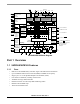

56F8365/56F8165 Features
56F8365 Technical Data, Rev. 9
Freescale Semiconductor 7
— In the 56F8365, two Pulse Width Modulator modules, each with six PWM outputs, three Current Sense
inputs, and four Fault inputs; fault-tolerant design with dead time insertion; supports both center-aligned
and edge-aligned modes
— In the 56F8165, one Pulse Width Modulator module with six PWM outputs, three Current Sense inputs
and three Fault inputs; fault-tolerant design with dead time insertion; supports both center-aligned and
edge-aligned modes
• Four 12-bit, Analog-to-Digital Converters (ADCs), which support four simultaneous conversions with
quad, 4-pin multiplexed inputs; ADC and PWM modules can be synchronized through Timer C, channels
2 and 3
• Quadrature Decoder:
— In the 56F8365, two four-input Quadrature Decoders or two additional Quad Timers
— In the 56F8165, one four-input Quadrature Decoder, which works in conjunction with Quad Timer A
• Temperature Sensor can be connected, on the board, to any of the ADC inputs to monitor the on-chip
temperature
•Quad Timer:
— In the 56F8365, four dedicated general-purpose Quad Timers totaling six dedicated pins: Timer C with
two pins and Timer D with four pins
— In the 56F8165, two Quad Timers; Timer A and Timer C both work in conjunction with GPIO
• Optional On-Chip Regulator
• Up to two FlexCAN (CAN Version 2.0 B-compliant) modules with 2-pin port for transmit and receive
• Two Serial Communication Interfaces (SCIs), each with two pins (or four additional GPIO lines)
• Up to two Serial Peripheral Interfaces (SPIs), both with configurable 4-pin port (or eight additional GPIO
lines); SPI1 can also be used as Quadrature Decoder 1 or Quad Timer B
• Computer Operating Properly (COP)/Watchdog timer
• Two dedicated external interrupt pins
• 49 General Purpose I/O (GPIO) pins; 28 pins dedicated to GPIO
• External reset input pin for hardware reset
• External reset output pin for system reset
• Integrated low-voltage interrupt module
• JTAG/Enhanced On-Chip Emulation (OnCE) for unobtrusive, processor speed-independent, real-time
debugging
• Software-programmable, Phase Lock Loop (PLL)-based frequency synthesizer for the core clock
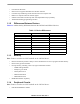
1.1.5 Energy Information
• Fabricated in high-density CMOS with 5V-tolerant, TTL-compatible digital inputs
• On-board 3.3V down to 2.6V voltage regulator for powering internal logic and memories; can be disabled
• On-chip regulators for digital and analog circuitry to lower cost and reduce noise
• Wait and Stop modes available
• ADC smart power management
• Each peripheral can be individually disabled to save power