Freescale Semiconductor Data Sheet: Technical Data Document Number: MCF51AC256 Rev.7, 9/2011 MCF51AC256 MCF51AC256 Series ColdFire Microcontroller 80 LQFP 14 mm 14 mm Covers:MCF51AC256A MCF51AC256B MCF51AC128A MCF51AC128C The MCF51AC256 series are members of the ColdFire® family of 32-bit variable-length reduced instruction set (RISC) microcontroller. This document provides an overview of the MCF51AC256 series, focusing on its highly integrated and diverse feature set.
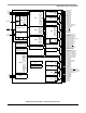
Table of Contents 1 2 3 4 MCF51AC256 Family Configurations . . . . . . . . . . . . . . . . . . . .3 1.1 Device Comparison. . . . . . . . . . . . . . . . . . . . . . . . . . . . .3 1.2 Block Diagram. . . . . . . . . . . . . . . . . . . . . . . . . . . . . . . . .4 1.3 Features . . . . . . . . . . . . . . . . . . . . . . . . . . . . . . . . . . . . .6 1.3.1 Feature List . . . . . . . . . . . . . . . . . . . . . . . . . . . . .7 1.4 Part Numbers . . . . . . . . . . . . . . . . . . . . . . . . . . . . . . .
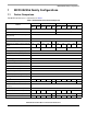
MCF51AC256 Family Configurations 1 MCF51AC256 Family Configurations 1.1 Device Comparison The MCF51AC256 series is summarized in Table 1. Table 1.
MCF51AC256 Family Configurations Table 1. MCF51AC256 Series Device Comparison (continued) MCF51AC256A MCF51AC256B 80-pin 64-pin 80-pin 64-pin 44-pin MCF51AC128A MCF51AC128C Feature TPM3 (timer pulse-width modulator) channels 2 64-pin 80-pin No Yes 64-pin 44-pin 2 VBUS (debug visibility bus) 1 80-pin Yes No Yes No Yes No The members of MCF51AC128A with CAN support have 32 KB RAM. The other members have 16 KB RAM.
TPMCLK ColdFire V1 core RESET FTM1 SIM IRQ/ TPMCLK TPMCLK COP LVD IRQ FTM2 FLASH MCF51AC256A/B = 256 KB MCF51AC128A/C = 128 KB TPMCLK TPM3 RAM VDD VSS VSS Port F: FTM1CH5 FTM1CH4 FTM1CH3 FTM1CH2 Port E: FTM1CH1 FTM1CH0 Port H: FTM2CH5 FTM2CH4 FTM2CH3 FTM2CH2 Port F: FTM2CH1 FTM2CH0 KBI MCG OSC Port G: KBI1P4 KBI1P3 KBI1P2 KBI1P1 KBI1P0 Port D: KBI1P7 KBI1P6 KBI1P5 Port G: EXTAL XTAL Port B Port C: SDA1 SCL1 LPO Port B: TPM3CH1 TPM3CH0 Port A: RxCAN TxCAN Port F Port F: RGPIO15 RGPIO1
MCF51AC256 Family Configurations 1.3 Features Table 2 describes the functional units of the MCF51AC256 series. Table 2.
MCF51AC256 Family Configurations 1.3.1 • • • • • • • Feature List 32-bit Version 1 ColdFire® central processor unit (CPU) — Up to 50.33 MHz at 2.7 V – 5.5 V — Provide 0.94 Dhrystone 2.1 DMIPS per MHz performance when running from internal RAM (0.
MCF51AC256 Family Configurations • • • • • — Trimmable internal reference allows 0.
MCF51AC256 Family Configurations • • • • Inter-integrated circuit (IIC) — Compatible with IIC bus standard — Multi-master operation — Software programmable for one of 64 different serial clock frequencies — Interrupt driven byte-by-byte data transfer — Arbitration lost interrupt with automatic mode switching from master to slave — Calling address identification interrupt — Bus busy detection — 10-bit address extension Controller area network (CAN) — Implementation of the CAN protocol — Version 2.
MCF51AC256 Family Configurations • 1.
MCF51AC256 Family Configurations Table 3.
MCF51AC256 Family Configurations 1.
64 63 62 61 60 59 58 57 56 55 54 53 52 51 50 49 PTC5 / RxD2 PTC3 / TxD2 PTC2 / MCLK PTC1 / SDA1 PTC0 / SCL1 VSS PTG6 / EXTAL PTG5 / XTAL BKGD / MS VREFL VREFH PTD7 / KBI1P7 / AD1P15 PTD6 / FTM1CLK / AD1P14 PTD5 / AD1P13 PTD4 / FTM2CLK / AD1P12 PTG4 / KBI1P4 / AD1P19 MCF51AC256 Family Configurations 1 2 3 4 5 6 7 8 9 10 11 12 13 14 15 16 64-Pin QFP 64-Pin LQFP 48 47 46 45 44 43 42 41 40 39 38 37 36 35 34 33 PTG3 / KBI1P3 / AD1P18 PTD3 / KBI1P6 / AD1P11 PTD2 / KBI1P5 / AD1P10 /ACMP1O VSSA VDDA PTD1 / AD
PTC2/MCLK PTC1/SDA1 PTC0/SCL1 VSS PTG6/EXTAL PTG5/XTAL BKGD/MS VREFL 43 42 41 40 39 38 37 36 35 34 44 PTC4 1 VREFH PTC3/TxD2 PTC5/RxD2 MCF51AC256 Family Configurations 33 PTG3/KBI1P3/AD1P18 IRQ/TPMCLK 2 32 PTD3/KBI1P6/AD1P11 RESET 3 31 PTD2/KBI1P5/AD1P10/ACMP1O PTF0/RGPIO8/FTM1CH2 4 30 VSSA PTF1/RGPIO9/FTM1CH3 5 29 VDDA 28 PTD1/AD1P9/ACMP1- 44-Pin LQFP PTF4/RGPIO12/FTM2CH0 6 PTF5/RGPIO13/FTM2CH1 7 27 PTD0/AD1P8/ACMP1+ PTE0/RGPIO0/TxD1 8 26 PTB3/AD1P3 PTE1
MCF51AC256 Family Configurations Table 4.
MCF51AC256 Family Configurations Table 4.
Electrical Characteristics 2 Electrical Characteristics This section contains electrical specification tables and reference timing diagrams for the MCF51AC256 microcontroller, including detailed information on power considerations, DC/AC electrical characteristics, and AC timing specifications. The electrical specifications are preliminary and are from previous designs or design simulations. These specifications may not be fully tested or guaranteed at this early stage of the product life cycle.
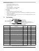
Electrical Characteristics Table 6. Absolute Maximum Ratings Rating Symbol Value Unit Supply voltage VDD –0.3 to 5.8 V Input voltage VIn –0.3 to VDD + 0.3 V Instantaneous maximum current Single pin limit (applies to all port pins)1, 2, 3 ID 25 mA Maximum current into VDD IDD 120 mA Storage temperature Tstg –55 to 150 C 1 Input must be current limited to the value specified.
Electrical Characteristics 1 Junction temperature is a function of die size, on-chip power dissipation, package thermal resistance, mounting site (board) temperature, ambient temperature, air flow, power dissipation of other components on the board, and board thermal resistance 2 Junction to Ambient Natural Convection 3 1s — Single layer board, one signal layer 4 2s2p — Four layer board, 2 signal and 2 power layers The average chip-junction temperature (TJ) in C can be obtained from: TJ = TA + (PD JA)
Electrical Characteristics applicable device specification at room temperature followed by hot temperature, unless specified otherwise in the device specification. Table 8.
Electrical Characteristics Table 10. DC Characteristics (continued) Num C 3 P Parameter Symbol Output low voltage — Low Drive (PTxDSn = 0) 5 V, ILoad = 4 mA 3 V, ILoad = 2 mA 5 V, ILoad = 2 mA 3 V, ILoad = 1 mA Output low voltage — High Drive (PTxDSn = 1) 5 V, ILoad = 15 mA 3 V, ILoad = 8 mA 5 V, ILoad = 8 mA 3 V, ILoad = 4 mA Min — Typical1 Max — 1.5 1.5 0.8 0.8 VOL — — 1.5 1.5 0.8 0.
Electrical Characteristics Table 10. DC Characteristics (continued) Num C Parameter DC injection current5 6 7 8 Symbol 2 3 4 5 6 7 8 Max Unit 0 0 — 2 –0.2 mA D DC injection current (Total MCU limit, includes sum of all stressed pins) VIN >VDD VIN
Electrical Characteristics –20.0E-3 VDD–VOH (V) Average of IOH –18.0E-3 –16.0E-3 –14.0E-3 –12.0E-3 –10.0E-3 –8.0E-3 –6.0E-3 -40C 25C IOH (A) 105C –4.0E-3 –2.0E-3 000E+0 0 0.3 0.5 0.8 VSupply–VOH 0.9 1.2 1.5 Figure 6. Typical IOH vs. VDD–VOH at VDD = 3 V (High Drive, PTxDSn = 1) VDD–VOH (V) Average of IOH –7.0E-3 –6.0E-3 -40C 25C –5.0E-3 105C IOH (A) –4.0E-3 –3.0E-3 –2.0E-3 –1.0E-3 000E+0 0.00 0.30 0.50 0.80 1.00 1.30 2.00 VSupply–VOH Figure 7. Typical IOH vs.
Electrical Characteristics –30.0E-3 VDD–VOH (V) Average of IOH -40C 25C –20.0E-3 105C IOH (A) –25.0E-3 –15.0E-3 –10.0E-3 –5.0E-3 000E+0 0.00 0.30 0.50 0.80 1.00 1.30 2.00 VSupply–VOH Figure 8. Typical IOH vs. VDD–VOH at VDD = 5 V (High Drive, PTxDSn = 1) MCF51AC256 ColdFire Microcontroller Data Sheet, Rev.
Electrical Characteristics 2.6 Supply Current Characteristics Table 11.
Electrical Characteristics Table 11. Supply Current Characteristics (continued) Num C Parameter Symbol 5 C Wait mode supply3 current measured at (CPU clock = 2 MHz, fBus = 1 MHz) 6 C Wait mode supply3 current measured at (CPU clock = 16 MHz, fBus = 8 MHz) 7 C Wait mode supply3 current measured at (CPU clock = 50 MHz, fBus = 25 MHz) WIDD VDD (V) Typical1 Max2 5 1.3 2 3 1.29 2 5 5.11 8 3 5.1 8 5 15.24 25 3 15.2 25 5 1.40 3 1.16 5 1.60 3 1.
Electrical Characteristics Figure 9. Typical Run IDD vs. System Clock Freq. for FEI and FBE Modes 2.7 Analog Comparator (ACMP) Electricals Table 12. Analog Comparator Electrical Specifications Num C Rating Symbol Min Typical Max Unit 1 — Supply voltage VDD 2.7 — 5.5 V 2 T Supply current (active) IDDAC — 20 35 A 3 D Analog input voltage VAIN VSS – 0.3 — VDD V 4 D Analog input offset voltage VAIO — 20 40 mV 5 D Analog comparator hysteresis VH 3.0 6.0 20.
Electrical Characteristics 2.8 ADC Characteristics Table 13. 5 Volt 12-bit ADC Operating Conditions Num C Characteristic D 1 Symb Min Typical1 Max Unit Absolute VDDA 2.7 — 5.5 V Delta to VDD (VDD – VDDA)2 VDDA –100 0 100 mV Delta to VSS (VSS – VSSA)2 VSSA –100 0 100 mV Conditions Supply voltage D 2 D Ground voltage 3 D Reference voltage high VREFH 2.
Electrical Characteristics SIMPLIFIED INPUT PIN EQUIVALENT CIRCUIT RAS CAS + – SIMPLIFIED CHANNEL SELECT CIRCUIT Pad leakage due to input protection ZAS VAS ZADIN RADIN ADC SAR ENGINE + VADIN – RADIN INPUT PIN RADIN INPUT PIN RADIN INPUT PIN CADIN Figure 10. ADC Input Impedance Equivalency Diagram Table 14.
Electrical Characteristics Table 14. 5 Volt 12-bit ADC Characteristics (VREFH = VDDA, VREFL = VSSA) (continued) Min Typical1 Max — 20 — — 40 — — 3.5 — — 23.5 — — 3.0 — — 1 2.5 8-bit mode — 0.5 1.0 12-bit mode — 1.75 — — 0.5 1.
Electrical Characteristics 3 4 Monotonicity and No-Missing-Codes guaranteed in 10-bit and 8-bit modes Based on input pad leakage current. Refer to pad electricals. 2.9 External Oscillator (XOSC) Characteristics Table 15.
Electrical Characteristics MCU EXTAL XTAL RS RF C1 2.10 Crystal or Resonator C2 MCG Specifications Table 16. MCG Frequency Specifications (Temperature Range = –40 to 105 C Ambient) Num C Rating Internal reference frequency — factory trimmed at VDD = 5 V and temperature = 25 C Symbol Min Typical1 Max Unit fint_ft — 32.768 — kHz 31.25 — 39.
Electrical Characteristics Table 16. MCG Frequency Specifications (continued)(Temperature Range = –40 to 105 C Ambient) Num C 18 1 2 3 4 5 6 7 8 Rating D Lock exit frequency tolerance 8 Symbol Min Typical1 Dunl 4.47 Max Unit — 5.
Electrical Characteristics 2.11.1 Control Timing Table 17.
Electrical Characteristics 2.11.2 Timer (TPM/FTM) Module Timing Synchronizer circuits determine the shortest input pulses that can be recognized or the fastest clock that can be used as the optional external source to the timer counter. These synchronizers operate from the current bus rate clock. Table 18.
Electrical Characteristics 2.12 SPI Characteristics Table 20 and Figure 15 through Figure 18 describe the timing requirements for the SPI system. Table 20. SPI Timing No.
Electrical Characteristics SS1 (OUTPUT) 11 1 2 SPSCK (CPOL = 0) (OUTPUT) 3 4 4 12 SPSCK (CPOL = 1) (OUTPUT) 5 MISO (INPUT) 6 MSB IN2 BIT 6 . . . 1 9 MOSI (OUTPUT) LSB IN 10 9 MSB OUT2 BIT 6 . . . 1 LSB OUT NOTES: 1. SS output mode (DDS7 = 1, SSOE = 1). 2. LSBF = 0. For LSBF = 1, bit order is LSB, bit 1, ..., bit 6, MSB. Figure 15.
Electrical Characteristics SS (INPUT) 1 12 11 11 12 3 SPSCK (CPOL = 0) (INPUT) 2 4 4 SPSCK (CPOL = 1) (INPUT) 8 7 MISO (OUTPUT) SLAVE LSB OUT SEE NOTE 6 5 MOSI (INPUT) BIT 6 . . . 1 MSB OUT SLAVE 10 10 9 BIT 6 . . . 1 MSB IN LSB IN NOTE: 1. Not defined but normally MSB of character just received Figure 17.
Electrical Characteristics Table 21. Flash Characteristics Symbol Min Typical1 Max Unit Supply voltage for program/erase Vprog/erase 2.7 — 5.5 V — Supply voltage for read operation VRead 2.7 — 5.5 V 3 — Internal FCLK frequency2 fFCLK 150 — 200 kHz 4 — Internal FCLK period (1/FCLK) tFcyc 5 — 6.
Mechanical Outline Drawings 3 Mechanical Outline Drawings Table 22 provides the available package types and their document numbers. The latest package outline/mechanical drawings are available on the MCF51AC256 Series Product Summary pages at http://www.freescale.com. To view the latest drawing, either: • Click on the appropriate link in Table 22, or • Open a browser to the FreescaleÆ website (http://www.freescale.
Revision History 4 Revision History Table 23. Revision History Revision Description 1 Initial published 2 Updated ADC channels, Item 1, 4-5 on Table 2.10 3 Completed all theTBDs. Changed RTC to RTI in Figure 1. Corrected the block diagram. Changed VDDAD to VDDA, VSSAD to VSSA. Added charge device model data and removed machine data in Table 8. Updated the specifications of VLVDH, VLVDL, VLVWH and VLVWL in Table 10. Updated S2IDD, S3IDD in Table 11. Added C column in Table 14.
How to Reach Us: Home Page: www.freescale.com Web Support: http://www.freescale.com/support USA/Europe or Locations Not Listed: Freescale Semiconductor, Inc. Technical Information Center, EL516 2100 East Elliot Road Tempe, Arizona 85284 1-800-521-6274 or +1-480-768-2130 www.freescale.