
Datasheet

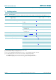

NPIC6C596A All information provided in this document is subject to legal disclaimers. © NXP B.V. 2013. All rights reserved.
Product data sheet Rev. 1 — 23 October 2013 10 of 21
NXP Semiconductors
NPIC6C596A
Power logic 8-bit shift register; open-drain outputs
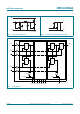
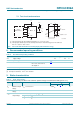
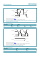
Measurement points are given in Table 7.
V
OL
and V
OH
are the typical output voltage levels that occur with the output load.
Fig 11. The shift clock (SHCP) to serial data output (Q7S) propagation delays with the minimum shift clock pulse
width and maximum shift clock frequency
aaa-002558
SHCP input
Q7S output
V
I
GND
V
OH
V
OL
1/f
max
t
PHL
V
M
V
M
t
PLH
t
W
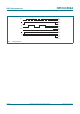
Table 7. Measurement points
Supply voltage Input Output
V
CC
V
M
V
M
V
X
V
Y
5 V 0.5V
CC
0.5V
DS
0.1V
DS
0.9V
DS
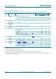
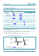
Measurement points are given in Table 8.
The shaded areas indicate when the input is permitted to change for predictable output performance.
V
OL
and V
OH
are the typical output voltage levels that occur with the output load.
Fig 12. The data set-up and hold times for the serial data input (DS)
aaa-002559
SHCP input
DS input
Q7S output
V
I
GND
V
I
GND
V
OH
V
OL
V
M
V
M
V
M
t
su
t
su
t
h
t
h
Table 8. Measurement points
Supply voltage Input Output
V
CC
V
M
V
M
5 V 0.5V
CC
0.5V
CC