
Datasheet


NPIC6C596A All information provided in this document is subject to legal disclaimers. © NXP B.V. 2013. All rights reserved.
Product data sheet Rev. 1 — 23 October 2013 6 of 21
NXP Semiconductors
NPIC6C596A
Power logic 8-bit shift register; open-drain outputs
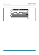
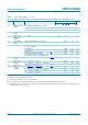
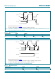
7. Limiting values
[1] Each power EDNMOS source is internally connected to GND.
[2] Pulse duration 100 s and duty cycle 2 %.
[3] V
DS
= 15 V; starting junction temperature (T
j
) = 25 C; L = 1.5 H; avalanche current (I
AL
) = 200 mA.
[4] For SO16 packages: above 25 C the value of P
tot
derates linearly with 6.4 mW/C.
For TSSOP16 packages: above 25 C the value of P
tot
derates linearly with 5.8 mW/C.
For DHVQFN16 packages: above 25 C the value of P
tot
derates linearly with 14.6 mW/C.
Table 3. Limiting values
In accordance with the Absolute Maximum Rating System (IEC 60134). Voltages are referenced to GND (ground = 0 V).
Symbol Parameter Conditions Min Max Unit
V
CC
supply voltage 0.5 +7.0 V
V
I
input voltage 0.3 +7.0 V
V
DS
drain-source voltage power EDNMOS drain-source
voltage
[1]
-+33 V
I
d(SD)
source-drain diode current continuous - 250 mA
pulsed
[2]
-500 mA
I
D
drain current T
amb
= 25 C
continuous; each output;
all outputs on
-100 mA
pulsed; each output;
all outputs on
[2]
-250 mA
I
DM
peak drain current single output; T
amb
= 25 C
[2]
-250 mA
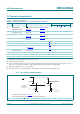
E
AS
non-repetitive avalanche energy single pulse; see Figure 9
[3]
-30 mJ
I
AL
avalanche current see Figure 9
[3]
-200 mA
T
stg
storage temperature 65 +150 C
P
tot
total power dissipation T
amb
= 25 C
[4]
SO16 - 800 mW
TSSOP16 - 725 mW
DHVQFN16 - 1825 mW
T
amb
= 125 C
[4]
SO16 - 160 mW
TSSOP16 - 145 mW
DHVQFN16 - 365 mW