
Datasheet


NPIC6C596A All information provided in this document is subject to legal disclaimers. © NXP B.V. 2013. All rights reserved.
Product data sheet Rev. 1 — 23 October 2013 8 of 21
NXP Semiconductors
NPIC6C596A
Power logic 8-bit shift register; open-drain outputs
[1] Typical values are measured at T
amb
= 25 C and V
CC
= 5.0 V.
[2] Output currents below 250 mA current limit.
[3] Technique should limit T
j
T
amb
to 10 C maximum.
[4] These parameters are measured with voltage-sensing contacts separate from the current-carrying contacts.
[5] Nominal output current is defined for a consistent comparison between devices from different sources. It is the current that produces a
voltage drop of 0.5 V at T
amb
= 85 C.
V
OL
LOW-level output
voltage
serial data output Q7S; V
I
=V
IH
or V
IL
I
O
=20A; V
CC
= 3.0 V - 0.005 0.12 V
I
O
=4mA; V
CC
= 3.0 V - 0.3 0.6 V
I
I
input leakage
current
V
CC
= 5.5 V; V
I
=V
CC
--1A
V
(BR)DSS
drain-source
breakdown
voltage
I
D
= 1 mA 33 37 - V
V
SD
source-drain
voltage
diode forward voltage; I
F
= 100 mA - 0.85 1.2 V
I
CC
supply current logic supply current; V
CC
= 5.5 V;
V
I
=V
CC
or GND
all outputs off - 0.004 200 A
all outputs on
[2]
- 0.006 500 A
all outputs off; SHCP = 5 MHz;
C
L
=30pF; see Figure 14 and Figure 16
-0.755mA
I
O(nom)
nominal output
current
V
DS
= 0.5 V; T
amb
=85C; I
out
= I
D
[3]
[4][5]
- 140 - mA
I
DSX
drain cut-off
current
V
CC
= 5.5 V; V
DS
= 30 V - 0.002 0.2 A
V
CC
= 5.5 V; V
DS
= 30 V; T
amb
= 125 C - 0.15 0.3 A
R
DSon
drain-source
on-state
resistance
see Figure 17 and Figure 18
[3][4]
V
CC
= 3.0 V; I
D
= 50 mA - 3.0 11
V
CC
= 3.0 V; I
D
= 50 mA; T
amb
= 125 C5.414
V
CC
= 3.0 V; I
D
= 100 mA - 3.1 12
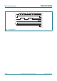
Table 5. Static characteristics
…continued
At recommended operating conditions unless otherwise specified. Voltages are referenced to GND (ground = 0 V).
Symbol Parameter Conditions T
amb
= 25 C Unit
Min Typ
[1]
Max