
Datasheet


NPIC6C596A All information provided in this document is subject to legal disclaimers. © NXP B.V. 2013. All rights reserved.
Product data sheet Rev. 1 — 23 October 2013 9 of 21
NXP Semiconductors
NPIC6C596A
Power logic 8-bit shift register; open-drain outputs
10. Dynamic characteristics
[1] Typical values are measured at T
amb
= 25 C and V
CC
= 5.0 V.
[2] t
pd
is the same as t
PLH
and t
PHL
.
[3] This is the maximum serial clock frequency assuming cascaded operation where serial data is passed from one stage to a second
stage. The clock period allows for SHCP → Q7S propagation delay and setup time plus some timing margin.
[4] Technique should limit T
j
T
amb
to 10 C maximum.
[5] These parameters are measured with voltage-sensing contacts separate from the current-carrying contacts.
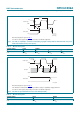
10.1 Test circuits and waveforms
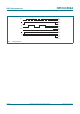
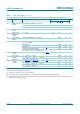
Table 6. Dynamic characteristics
Voltages are referenced to GND (ground = 0 V); For test circuit, see Figure 14.
Symbol Parameter Conditions T
amb
= 25 C Unit
Min Typ
[1]
Max
t
PLH
LOW to HIGH
propagation delay
OE to Qn; I
D
= 75 mA; see Figure 10 and
Figure 19
-97-ns
t
PHL
HIGH to LOW
propagation delay
OE to Qn; I
D
= 75 mA; see Figure 10 and
Figure 19
-9-ns
t
r
rise time OE to Qn; I
D
= 75 mA; see Figure 10 and
Figure 19
-60-ns
t
f
fall time OE to Qn; I
D
= 75 mA; see Figure 10 and
Figure 19
-18-ns
t
pd
propagation delay SHCP to Q7S; I
D
= 75 mA; see Figure 11
[2]
-5-ns
f
max
maximum frequency SHCP; I
D
= 75 mA; see Figure 11
[3]
--10MHz
t
rr
reverse recovery time I
F
= 100 mA; dI/dt = 10 A/s;
see Figure 13
[4][5]
- 120 - ns
t
a
reverse recovery
current rise time
I
F
= 100 mA; dI/dt = 10 A/s;
see Figure 13
[4][5]
- 100 - ns
t
su
set-up time DS to SHCP; see Figure 12 15 - - ns
t
h
hold time DS to SHCP; see Figure 12 15 - - ns
t
W
pulse width 40 - - ns
Measurement points are given in Table 7.
V
OL
is the typical output voltage drop that occurs with the output load.
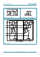
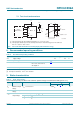
Fig 10. The output enable (OE) input to data output (Qn) propagation delays and (Qn) output rise and fall times
GND
24 V
t
PLH
t
r
V
M
V
I
V
OL
V
X
V
X
V
Y
t
PHL
t
f
V
Y
Qn output
LOW-to-OFF
OFF-to-LOW
OE input
aaa-002557