
Datasheet


NPIC6C596A_Q100 All information provided in this document is subject to legal disclaimers. © NXP B.V. 2013. All rights reserved.
Product data sheet Rev. 1 — 18 October 2013 10 of 20
NXP Semiconductors NPIC6C596A-Q100
Power logic 8-bit shift register; open-drain outputs
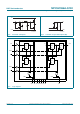
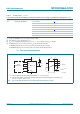
Measurement points are given in Table 8.
The shaded areas indicate when the input is permitted to change for predictable output performance.
V
OL
and V
OH
are the typical output voltage levels that occur with the output load.
Fig 12. The data set-up and hold times for the serial data input (DS)
aaa-002559
SHCP input
DS input
Q7S output
V
I
GND
V
I
GND
V
OH
V
OL
V
M
V
M
V
M
t
su
t
su
t
h
t
h
Table 8. Measurement points
Supply voltage Input Output
V
CC
V
M
V
M
5 V 0.5V
CC
0.5V
CC
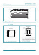
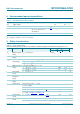
(1) The open-drain Qn terminal under test is connected to testpoint K. All other terminals are connected together and connected to
testpoint A.
(2) The V
I
amplitude and R
G
are adjusted for dI/dt = 10 A/s. A V
I
double-pulse train is used to set I
F
= 0.1 A, where t
1
= 10 s, t
2
=
7 s and t
3
= 3 s.
Fig 13. Test circuit and waveform for measuring reverse recovery current
aaa-002560
I
F
DUT
Qn
15 V
driver
R
G
G
50 Ω
2500 μF
250 V
0.85 mH
K
(1)
A
(1)
t
1
t
2
t
3
V
I
(2)
0.1 A
di/dt = 10 A/μs
I
F
t
a
t
rr
0
25 % of l
RM
I
RM