
Datasheet

NTS0101 All information provided in this document is subject to legal disclaimers. © NXP Semiconductors N.V. 2014. All rights reserved.
Product data sheet Rev. 5 — 11 August 2014 3 of 23
NXP Semiconductors
NTS0101
Dual supply translating transceiver; open drain; auto direction sensing
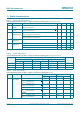
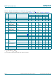
7. Pinning information
7.1 Pinning
7.2 Pin description
8. Functional description
[1] H = HIGH voltage level; L = LOW voltage level; X = don’t care; Z = high-impedance OFF-state.
[2] When either V
CC(A)
or V
CC(B)
is at GND level, the device goes into power-down mode.
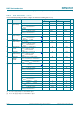
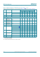
Fig 2. Pin configuration SOT363 Fig 3. Pin configuration SOT886 Fig 4. Pin configuration SOT891
and SOT1202
NTS0101
V
CC(A)
V
CC(B)
GND
AB
001aan318
1
2
3
6
OE
5
4
NTS0101
GND
001aan319
V
CC(A)
A
OE
V
CC(B)
B
Transparent top view
2
3
1
5
4
6
NTS0101
GND
001aan320
V
CC(A)
A
OE
V
CC(B)
B
Transparent top view
2
3
1
5
4
6
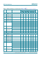
Table 3. Pin description
Symbol Pin Description
V
CC(A)
1 supply voltage A
GND 2 ground (0 V)
A 3 data input or output (referenced to V
CC(A)
)
B 4 data input or output (referenced to V
CC(B)
)
OE 5 output enable input (active HIGH; referenced to V
CC(A)
)
V
CC(B)
6 supply voltage B
Table 4. Function table
[1]
Supply voltage Input Input/output
V
CC(A)
V
CC(B)
OE A B
1.65 V to V
CC(B)
2.3 V to 5.5 V L Z Z
1.65 V to V
CC(B)
2.3 V to 5.5 V H input or output output or input
GND
[2]
GND
[2]
XZZ