
Datasheet

NTS0101 All information provided in this document is subject to legal disclaimers. © NXP Semiconductors N.V. 2014. All rights reserved.
Product data sheet Rev. 5 — 11 August 2014 7 of 23
NXP Semiconductors
NTS0101
Dual supply translating transceiver; open drain; auto direction sensing
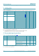
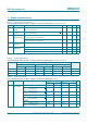
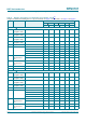
12. Dynamic characteristics
Table 10. Dynamic characteristics for temperature range 40 C to +85 C
[1]
Voltages are referenced to GND (ground = 0 V); for test circuit, see Figure 7; for wave forms, see Figure 5 and Figure 6.
Symbol Parameter Conditions V
CC(B)
Unit
2.5 V 0.2 V 3.3 V 0.3 V 5.0 V 0.5 V
Min Max Min Max Min Max
V
CC(A)
= 1.8 V 0.15 V
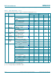
t
PHL
HIGH to LOW
propagation delay
A to B - 4.6 - 4.7 - 5.8 ns
t
PLH
LOW to HIGH
propagation delay
A to B - 6.8 - 6.8 - 7.0 ns
t
PHL
HIGH to LOW
propagation delay
B to A - 4.4 - 4.5 - 4.7 ns
t
PLH
LOW to HIGH
propagation delay
B to A - 5.3 - 4.5 - 0.5 ns
t
en
enable time OE to A; B - 200 - 200 - 200 ns
t
dis
disable time OE to A; no external load
[2]
-25-25-25ns
OE to B; no external load
[2]
-25-25-25ns
OE to A - 230 - 230 - 230 ns
OE to B - 200 - 200 - 200 ns
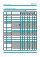
t
TLH
LOW to HIGH
output transition
time
A port 3.2 9.5 2.3 9.3 1.8 7.6 ns
B port 3.3 10.8 2.7 9.1 2.7 7.6 ns
t
THL
HIGH to LOW
output transition
time
A port 2.0 5.9 1.9 6.0 1.7 13.3 ns
B port 2.9 7.6 2.8 7.5 2.8 10.0 ns
t
W
pulse width data inputs 20 - 20 - 20 - ns
f
data
data rate - 50 - 50 - 50 Mbps
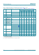
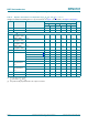
V
CC(A)
= 2.5 V 0.2 V
t
PHL
HIGH to LOW
propagation delay
A to B - 3.2 - 3.3 - 3.4 ns
t
PLH
LOW to HIGH
propagation delay
A to B - 3.5 - 4.1 - 4.4 ns
t
PHL
HIGH to LOW
propagation delay
B to A - 3.0 - 3.6 - 4.3 ns
t
PLH
LOW to HIGH
propagation delay
B to A - 2.5 - 1.6 - 0.7 ns
t
en
enable time OE to A; B - 200 - 200 - 200 ns
t
dis
disable time OE to A; no external load
[2]
-20-20-20ns
OE to B; no external load
[2]
-20-20-20ns
OE to A - 200 - 200 - 200 ns
OE to B - 200 - 200 - 200 ns
t
TLH
LOW to HIGH
output transition
time
A port 2.8 7.4 2.6 6.6 1.8 6.2 ns
B port 3.2 8.3 2.9 7.9 2.4 6.8 ns