
Datasheet


NVT2001_NVT2002 All information provided in this document is subject to legal disclaimers. © NXP B.V. 2014. All rights reserved.
Product data sheet Rev. 4 — 27 January 2014 2 of 26
NXP Semiconductors
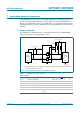
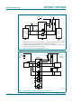
NVT2001; NVT2002
Bidirectional voltage level translator
Low 3.5 ON-state connection between input and output ports provides less signal
distortion
5 V tolerant I/O ports to support mixed-mode signal operation
High-impedance An and Bn pins for EN = LOW
Lock-up free operation
Flow through pinout for ease of printed-circuit board trace routing
ESD protection exceeds 4 kV HBM per JESD22-A114 and 1000 V CDM per
JESD22-C101
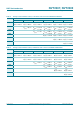
3. Ordering information
[1] GTL2002 = NVT2002.
[2] ‘X’ will change based on date code.
3.1 Ordering options
Table 1. Ordering information
T
amb
=
40
C to +85
C.
Type number Topside
marking
Number
of bits
Package
Name Description Version
NVT2002DP
[1]
N2002 2 TSSOP8 plastic thin shrink small outline package; 8 leads;
body width 3 mm
SOT505-1
NVT2002GD
[1]
N02 2 XSON8U plastic extremely thin small outline package; no leads;
8 terminals; UTLP based; body 3 2 0.5 mm
SOT996-2
NVT2001GM N1X
[2]
1 XSON6 plastic extremely thin small outline package; no leads;
6 terminals; body 1 1.45 0.5 mm
SOT886
Table 2. Ordering options
Type number Orderable
part number
Package Packing method Minimum
order
quantity
Temperature
NVT2002DP NVT2002DP,118 TSSOP8 Reel 13” Q1/T1
*Standard mark SMD
2500 T
amb
= 40 C to +85 C
NVT2002GD NVT2002GD,125 XSON8U Reel 7” Q3/T4
*Standard mark
3000 T
amb
= 40 C to +85 C
NVT2001GM NVT2001GM,115 XSON6 Reel 7” Q1/T1
*Standard mark SMD
5000 T
amb
= 40 C to +85 C