
Datasheet


NVT2001_NVT2002 All information provided in this document is subject to legal disclaimers. © NXP B.V. 2014. All rights reserved.
Product data sheet Rev. 4 — 27 January 2014 3 of 26
NXP Semiconductors
NVT2001; NVT2002
Bidirectional voltage level translator
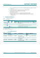
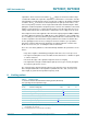
4. Functional diagram
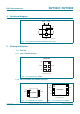
5. Pinning information
5.1 Pinning
5.1.1 1-bit in XSON6 package
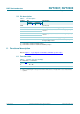
5.1.2 2-bit in TSSOP8 and XSON8U packages
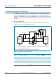
Fig 1. Logic diagram of NVT2001; NVT2002 (positive logic)
002aae132
A1
An
VREFA
GND
VREFB
B1
Bn
EN
SW
SW
NVT20xx
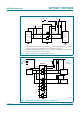
Fig 2. Pin configuration for XSON6
NVT2001GM
VREFA
002aae211
GND
A1
VREFB
EN
B1
Transparent top view
2
3
1
5
4
6
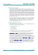
Fig 3. Pin configuration for TSSOP8 Fig 4. Pin configuration for XSON8U
NVT2002DP
GND EN
VREFA VREFB
A1 B1
A2 B2
002aae214
1
2
3
4
6
5
8
7
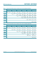
002aae215
NVT2002GD
Transparent top view
8
7
6
5
1
2
3
4
GND
VREFA
A1
A2
EN
VREFB
B1
B2