
Datasheet


NVT2001_NVT2002 All information provided in this document is subject to legal disclaimers. © NXP B.V. 2014. All rights reserved.
Product data sheet Rev. 4 — 27 January 2014 4 of 26
NXP Semiconductors
NVT2001; NVT2002
Bidirectional voltage level translator
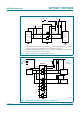
5.2 Pin description
[1] 1-bit NVT2001 available in XSON6 package.
[2] 2-bit NVT2002 available in TSSOP8 and XSON8U packages.
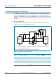
6. Functional description
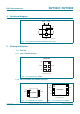
Refer to Figure 1 “Logic diagram of NVT2001; NVT2002 (positive logic)”.
6.1 Function table
[1] EN is controlled by the V
ref(B)
logic levels and should be at least 1 V higher than V
ref(A)
for best translator
operation.
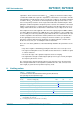
Table 3. Pin description
Symbol Pin Description
NVT2001
[1]
NVT2002
[2]
GND 1 1 ground (0 V)
VREFA 2 2 low-voltage side reference supply voltage for An
A1 3 3 low-voltage side; connect to VREFA through a pull-up
resistor
A2 - 4
B1 4 6 high-voltage side; connect to VREFB through a pull-up
resistor
B2 - 5
VREFB 5 7 high-voltage side reference supply voltage for Bn
EN 6 8 switch enable input; connect to VREFB and pull-up
through a high resistor
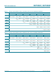
Table 4. Function selection (example)
H = HIGH level; L = LOW level.
Input EN
[1]
Function
HAn=Bn
L disconnect