
Datasheet


NVT2001_NVT2002 All information provided in this document is subject to legal disclaimers. © NXP B.V. 2014. All rights reserved.
Product data sheet Rev. 4 — 27 January 2014 5 of 26
NXP Semiconductors
NVT2001; NVT2002
Bidirectional voltage level translator
7. Application design-in information
The NVT2001/02 can be used in level translation applications for interfacing devices or
systems operating at different interface voltages with one another. The NVT2001/02 is
ideal for use in applications where an open-drain driver is connected to the data I/Os. The
NVT2001/02 can also be used in applications where a push-pull driver is connected to the
data I/Os.
7.1 Enable and disable
The NVT20xx has an EN input that is used to disable the device by setting EN LOW,
which places all I/Os in the high-impedance state.
[1] All typical values are at T
amb
=25C.
(1) The applied voltages at V
ref(A)
and V
pu(D)
should be such that V
ref(B)
is at least 1 V higher than
V
ref(A)
for best translator operation.
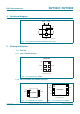
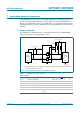
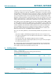
Fig 5. Typical application circuit (switch always enabled)
Table 5. Application operating conditions
Refer to Figure 5
.
Symbol Parameter Conditions Min Typ
[1]
Max Unit
V
ref(B)
reference voltage (B) V
ref(A)
+0.6 2.1 5 V
V
I(EN)
input voltage on pin EN V
ref(A)
+0.6 2.1 5 V
V
ref(A)
reference voltage (A) 0 1.5 4.4 V
I
sw(pass)
pass switch current - 14 - mA
I
ref
reference current transistor - 5 - A
T
amb
ambient temperature operating in
free-air
40 - +85 C
002aae134
A1
A2
VREFA
GND
3
4
VREFB
1
6
5
B1
B2
8EN
SW
SW
NVT2002
7
200 kΩ
R
PU
R
PU
V
pu(D)
= 3.3 V
(1)
I
2
C-BUS
DEVICE
SCL
SDA
V
CC
GND
2
V
ref(A)
= 1.8 V
(1)
R
PU
R
PU
I
2
C-BUS
MASTER
SCL
SDA
V
CC
GND