
Datasheet


NVT2008_NVT2010 All information provided in this document is subject to legal disclaimers. © NXP B.V. 2014. All rights reserved.
Product data sheet Rev. 3 — 27 January 2014 11 of 33
NXP Semiconductors
NVT2008; NVT2010
Bidirectional voltage-level translator
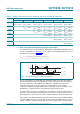
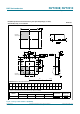
7.5 How to design for maximum frequency operation
The maximum frequency is limited by the minimum pulse width LOW and HIGH as well as
rise time and fall time. See Equation 1
as an example of the maximum frequency. The rise
and fall times are shown in Figure 11
.
(1)
The rise and fall times are dependent upon translation voltages, the drive strength, the
total node capacitance (C
L(tot)
) and the pull-up resistors (R
PU
) that are present on the bus.
The node capacitance is the addition of the PCB trace capacitance and the device
capacitance that exists on the bus. Because of the dependency of the external
components, PCB layout and the different device operating states the calculation of rise
and fall times is complex and has several inflection points along the curve.
The main component of the rise and fall times is the RC time constant of the bus line when
the device is in its two primary operating states: when device is in the ON state and it is
low-impedance, the other is when the device is OFF isolating the A-side from the B-side.
A description of the fall time applied to either An or Bn output going from HIGH to LOW is
as follows. Whichever side is asserted first, the B-side down must discharge to the V
CC(A)
voltage. The time is determined by the pull-up resistor, pull-down driver strength and the
Table 8. Pull-up resistor minimum values, 15 mA driver sink current for PCA9306 and NVT20xx
A-side B-side
1.2 V 1.5 V 1.8 V 2.5 V 3.3 V 5.0 V
1.0 V R
pu(A)
= 147
R
pu(B)
= 147
R
pu(A)
=169
R
pu(B)
=169
R
pu(A)
= 191
R
pu(B)
= 191
R
pu(A)
= none
R
pu(B)
=178
R
pu(A)
= none
R
pu(B)
= 237
R
pu(A)
= none
R
pu(B)
=365
1.2 V R
pu(A)
=182
R
pu(B)
=182
R
pu(A)
= 205
R
pu(B)
= 205
R
pu(A)
= none
R
pu(B)
=178
R
pu(A)
= none
R
pu(B)
= 237
R
pu(A)
= none
R
pu(B)
=365
1.5 V R
pu(A)
= 221
R
pu(B)
= 221
R
pu(A)
= none
R
pu(B)
=174
R
pu(A)
= none
R
pu(B)
= 232
R
pu(A)
= none
R
pu(B)
=357
1.8 V R
pu(A)
=294
R
pu(B)
=294
R
pu(A)
= none
R
pu(B)
= 232
R
pu(A)
= none
R
pu(B)
=357
2.5 V R
pu(A)
= 392
R
pu(B)
= 392
R
pu(A)
= none
R
pu(B)
=357
3.3 V R
pu(A)
= none
R
pu(B)
=348
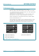
Fig 11. An example waveform for maximum frequency
f
max
1
t
LOW min
t
HIGH mi n
t
r actual
t
f actual
+++
-------------------------------------------------------------------------------------------------------------
=
002aag912
t
r(actual)
t
f(actual)
GND
V
OL
V
IL
V
IH
V
CC
t
HIGH(min)
t
LOW(min)
1 / f
max
0.9 × V
CC
0.1 × V
CC