
Datasheet


NVT2008_NVT2010 All information provided in this document is subject to legal disclaimers. © NXP B.V. 2014. All rights reserved.
Product data sheet Rev. 3 — 27 January 2014 12 of 33
NXP Semiconductors
NVT2008; NVT2010
Bidirectional voltage-level translator
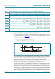
capacitance. As the level moves below the V
CC(A)
voltage, the channel resistance drops
so that both A and B sides equal. The capacitance on both sides is connected to form the
total capacitance and the pull-up resistors on both sides combine to the parallel equivalent
resistance. The R
on
of the device is small compared to the pull-up resistor values, so its
effect on the pull-up resistance can be neglected and the fall is determined by the driver
pulling the combined capacitance and pull-up resistor currents. An estimation of the actual
fall time seen by the device is equal to the time it takes for the B-side to fall to the V
CC(A)
voltage and the time it takes for both sides to fall from the V
CC(A)
voltage to the V
IL
level.
A description of the rise time applied to either An or Bn output going from LOW to HIGH is
as follows. When the signal level is LOW, the R
on
is at its minimum, so the A and B sides
are essentially one node. They will rise together with an RC time constant that is the sum
of all the capacitance from both sides and the parallel of the resistance from both sides.
As the signal approaches the V
CC(A)
voltage, the channel resistance goes up and the
waveforms separate, with the B side finishing its rise with the RC time constant of the
B side. The rise to V
CC(A)
is essentially the same for both sides.
There are some basic guidelines to follow that will help maximize the performance of the
device:
• Keep trace length to a minimum by placing the NVT device close to the processor.
• The signal round trip time on trace should be shorter than the rise or fall time of signal
to reduce reflections.
• The faster the edge of the signal, the higher the chance for ringing.
• The higher drive strength controlled by the pull-up resistor (up to 15 mA), the higher
the frequency the device can use.
The system designer must design the pull-up resistor value based on external current
drive strength and limit the node capacitance (minimize the wire, stub, connector and
trace length) to get the desired operation frequency result.
8. Limiting values
[1] The input and input/output negative voltage ratings may be exceeded if the input and input/output clamp
current ratings are observed.
[2] Low duty cycle pulses, not DC because of heating.
Table 9. Limiting values
In accordance with the Absolute Maximum Rating System (IEC 60134).
Over operating free-air temperature range.
Symbol Parameter Conditions Min Max Unit
V
ref(A)
reference voltage (A) 0.5 +6 V
V
ref(B)
reference voltage (B) 0.5 +6 V
V
I
input voltage 0.5
[1]
+6 V
V
I/O
voltage on an input/output pin 0.5
[1]
+6 V
I
ch
channel current (DC) - 128 mA
I
IK
input clamping current V
I
<0V 50 - mA
I
OK
output clamping current
[2]
50 +50 mA
T
stg
storage temperature 65 +150 C