
Datasheet


NVT2008_NVT2010 All information provided in this document is subject to legal disclaimers. © NXP B.V. 2014. All rights reserved.
Product data sheet Rev. 3 — 27 January 2014 15 of 33
NXP Semiconductors
NVT2008; NVT2010
Bidirectional voltage-level translator
11. Dynamic characteristics
11.1 Open-drain drivers
[1] See graphs based on R
on
typical and C
io(on)
+C
L
=50pF.
Table 12. Dynamic characteristics for open-drain drivers
T
amb
=
40
Cto+85
C; V
I(EN)
=V
ref(B)
; R
bias(ext)
= 200 k
; C
VREFB
=0.1
F; unless otherwise
specified.
Symbol Parameter Conditions Min Typ Max Unit
Refer to Figure 15
t
PLH
LOW to HIGH
propagation delay
from (input) Bn
to (output) An
[1]
R
on
(C
L
+ C
io(on)
)ns
t
PHL
HIGH to LOW
propagation delay
from (input) Bn
to (output) An
R
on
(C
L
+ C
io(on)
)ns
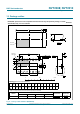
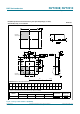
Fig 13. AC test setup Fig 14. Example of typical AC waveform
002aaf347
DUT
EN VREFB
VREFA
1.5 V
200 kΩ
SIGNAL
GENERATOR
5.5 V
0.1 μF
1.5 V swing
50 pF
450 Ω
500 Ω
6.6 V
1 V/div
40 ns/div
002aaf348
Bn
An
GND
GND
a. Load circuit b. Timing diagram; high-impedance scope probe
used
S2 = translating down, and same voltage.
C
L
includes probe and jig capacitance.
All input pulses are supplied by generators having the following characteristics: PRR 10 MHz; Z
o
=50; t
r
2ns; t
f
2ns.
The outputs are measured one at a time, with one transition per measurement.
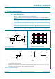
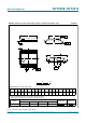
Fig 15. Load circuit for outputs
002aab845
V
TT
R
L
S1
S2 (open)
C
L
from output under test
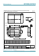
002aab846
V
IH
V
IL
V
M
V
M
input
output
V
OH
V
OL
V
M
V
M