
Datasheet


NXP Semiconductors
NVT2008; NVT2010
Bidirectional voltage-level translator
© NXP B.V. 2014. All rights reserved.
For more information, please visit: http://www.nxp.com
For sales office addresses, please send an email to: salesaddresses@nxp.com
Date of release: 27 January 2014
Document identifier: NVT2008_NVT2010
Please be aware that important notices concerning this document and the product(s)
described herein, have been included in section ‘Legal information’.
21. Contents
1 General description. . . . . . . . . . . . . . . . . . . . . . 1
2 Features and benefits . . . . . . . . . . . . . . . . . . . . 1
3 Ordering information. . . . . . . . . . . . . . . . . . . . . 2
3.1 Ordering options . . . . . . . . . . . . . . . . . . . . . . . . 2
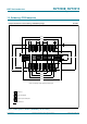
4 Functional diagram . . . . . . . . . . . . . . . . . . . . . . 3
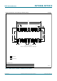
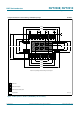
5 Pinning information. . . . . . . . . . . . . . . . . . . . . . 3
5.1 Pinning . . . . . . . . . . . . . . . . . . . . . . . . . . . . . . . 3
5.1.1 8-bit in TSSOP20 and DHVQFN20 packages . 3
5.1.2 10-bit in TSSOP24, DHVQFN24 and HVQFN24
packages . . . . . . . . . . . . . . . . . . . . . . . . . . . . . 4
5.2 Pin description . . . . . . . . . . . . . . . . . . . . . . . . . 5
6 Functional description . . . . . . . . . . . . . . . . . . . 6
6.1 Function table . . . . . . . . . . . . . . . . . . . . . . . . . . 6
7 Application design-in information . . . . . . . . . . 6
7.1 Enable and disable . . . . . . . . . . . . . . . . . . . . . . 6
7.2 Bidirectional translation . . . . . . . . . . . . . . . . . . 8
7.3 Bidirectional level shifting between two different
power domains nominally at the same potential 9
7.4 How to size pull-up resistor value. . . . . . . . . . . 9
7.5 How to design for maximum frequency
operation. . . . . . . . . . . . . . . . . . . . . . . . . . . . . 11
8 Limiting values. . . . . . . . . . . . . . . . . . . . . . . . . 12
9 Recommended operating conditions. . . . . . . 13
10 Static characteristics. . . . . . . . . . . . . . . . . . . . 13
11 Dynamic characteristics . . . . . . . . . . . . . . . . . 15
11.1 Open-drain drivers . . . . . . . . . . . . . . . . . . . . . 15
12 Performance curves . . . . . . . . . . . . . . . . . . . . 16
13 Package outline . . . . . . . . . . . . . . . . . . . . . . . . 17
14 Soldering of SMD packages . . . . . . . . . . . . . . 22
14.1 Introduction to soldering . . . . . . . . . . . . . . . . . 22
14.2 Wave and reflow soldering . . . . . . . . . . . . . . . 22
14.3 Wave soldering. . . . . . . . . . . . . . . . . . . . . . . . 22
14.4 Reflow soldering. . . . . . . . . . . . . . . . . . . . . . . 23
15 Soldering: PCB footprints. . . . . . . . . . . . . . . . 25
16 Abbreviations. . . . . . . . . . . . . . . . . . . . . . . . . . 30
17 Revision history. . . . . . . . . . . . . . . . . . . . . . . . 30
18 Legal information. . . . . . . . . . . . . . . . . . . . . . . 31
19 Data sheet status . . . . . . . . . . . . . . . . . . . . . . 31
19.1 Definitions. . . . . . . . . . . . . . . . . . . . . . . . . . . . 31
19.2 Disclaimers . . . . . . . . . . . . . . . . . . . . . . . . . . . 31
19.3 Trademarks. . . . . . . . . . . . . . . . . . . . . . . . . . . 32
20 Contact information. . . . . . . . . . . . . . . . . . . . . 32
21 Contents . . . . . . . . . . . . . . . . . . . . . . . . . . . . . . 33