
Datasheet


NVT2008_NVT2010 All information provided in this document is subject to legal disclaimers. © NXP B.V. 2014. All rights reserved.
Product data sheet Rev. 3 — 27 January 2014 7 of 33
NXP Semiconductors
NVT2008; NVT2010
Bidirectional voltage-level translator
[1] All typical values are at T
amb
=25C.
Table 5. Application operating conditions
Refer to Figure 7.
Symbol Parameter Conditions Min Typ
[1]
Max Unit
V
ref(B)
reference voltage (B) V
ref(A)
+0.6 2.1 5 V
V
I(EN)
input voltage on pin EN V
ref(A)
+0.6 2.1 5 V
V
ref(A)
reference voltage (A) 0 1.5 4.4 V
I
sw(pass)
pass switch current - 14 - mA
I
ref
reference current transistor - 5 - A
T
amb
ambient temperature operating in
free-air
40 - +85 C
(1) In the Enabled mode, the applied enable voltage V
I(EN)
and the applied voltage at V
ref(A)
should be
such that V
ref(B)
is at least 1 V higher than V
ref(A)
for best translator operation.
(2) Note that the enable time and the disable time are essentially controlled by the RC time constant of
the capacitor and the 200 k resistor on the EN pin.
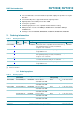
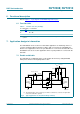
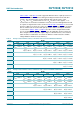
Fig 8. Typical application circuit (switch enable control)
002aae135
A1
A2
VREFA
GND
3
4
VREFB
1
6
5
B1
B2
8EN
SW
SW
NVT2002
7
200 kΩ
R
PU
R
PU
V
pu(D)
= 3.3 V
I
2
C-BUS
DEVICE
SCL
SDA
V
CC
GND
2
V
ref(A)
= 1.8 V
(1)
R
PU
R
PU
I
2
C-BUS
MASTER
SCL
SDA
V
CC
GND
on
off
3.3 V enable signal
(1)
(2)