
Datasheet


NVT2008_NVT2010 All information provided in this document is subject to legal disclaimers. © NXP B.V. 2014. All rights reserved.
Product data sheet Rev. 3 — 27 January 2014 9 of 33
NXP Semiconductors
NVT2008; NVT2010
Bidirectional voltage-level translator
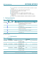
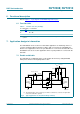
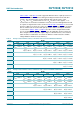
7.3 Bidirectional level shifting between two different power domains
nominally at the same potential
The less obvious application for the NVT2008/NVT2010 is for level shifting between two
different power domains that are nominally at the same potential, such as a 3.3 V system
where the line crosses power supply domains that under normal operation would be at
3.3 V, but one could be at 3.0 V and the other at 3.6 V, or one could be experiencing a
power failure while the other domain is trying to operate. One of the channel transistors is
used as a second reference transistor with its B side connected to a voltage supply that is
at least 1 V (and preferably 1.5 V) above the maximum possible for either V
pu(A)
or V
pu(B)
.
Then if either pull-up voltage is at 0 V, the channels are disabled, and otherwise the
channels are biased such that they turn OFF at the lower pull-up voltage, and if the two
pull-up voltages are equal, the channel is biased such that it just turns OFF at the
common pull-up voltage.
7.4 How to size pull-up resistor value
Sizing the pull-up resistor on an open-drain bus is specific to the individual application and
is dependent on the following driver characteristics:
• The driver sink current
• The V
OL
of driver
• The V
IL
of the driver
• Frequency of operation
The following tables can be used to estimate the pull-up resistor value in different use
cases so that the minimum resistance for the pull-up resistor can be found.
The applied enable voltage V
pu(H)
and the applied voltage at V
ref(A)
and V
ref(B)
should be such that V
ref(H)
is at least 1 V higher
than V
ref(A)
and V
ref(B)
for best translator operation.
Fig 10. Bidirectional level shifting between two different power domains
002aae967
A1
A2
VREFA
GND
3
4
VREFB
1
8
7
B1
B2
10 EN
SW
SW
NVT2003
9
200 kΩ
R
PU
R
PU
V
pu(B)
= 3.3 V
I
2
C-BUS
DEVICE
SCL
SDA
V
CC
GND
2
V
pu(A)
= 3.3 V
R
PU
R
PU
I
2
C-BUS
MASTER
SCL
SDA
V
CC
GND
V
pu(H)
A3 5 6
SW
B3
V
pu(B)