
Datasheet


PCA9306 All information provided in this document is subject to legal disclaimers. © NXP B.V. 2014. All rights reserved.
Product data sheet Rev. 8 — 22 January 2014 10 of 35
NXP Semiconductors
PCA9306
Dual bidirectional I
2
C-bus and SMBus voltage-level translator
11. Application information
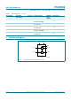
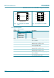
(1) The applied voltages at V
ref(1)
and V
pu(D)
should be such that V
bias(ref)(2)
is at least 1 V higher than
V
ref(1)
for best translator operation.
Fig 11. Typical application circuit (switch always enabled)
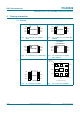
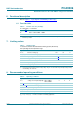
(1) In the Enabled mode, the applied enable voltage and the applied voltage at V
ref(1)
should be such
that V
bias(ref)(2)
is at least 1 V higher than V
ref(1)
for best translator operation.
Fig 12. Typical application circuit (switch enable control)
002aab847
SCL1
SDA1
VREF1
GND
3
4
VREF2
1
6
5
SCL2
SDA2
8EN
SW
SW
PCA9306
7
200 kΩ
R
PU
R
PU
V
pu(D)
= 3.3 V
(1)
I
2
C-BUS
DEVICE
SCL
SDA
V
CC
GND
2
V
ref(1)
= 1.8 V
(1)
R
PU
R
PU
I
2
C-BUS
MASTER
SCL
SDA
V
CC
GND
002aab848
SCL1
SDA1
VREF1
GND
3
4
VREF2
1
6
5
SCL2
SDA2
8EN
SW
SW
PCA9306
7
200 kΩ
R
PU
R
PU
V
pu(D)
= 3.3 V
I
2
C-BUS
DEVICE
SCL
SDA
V
CC
GND
2
V
ref(1)
= 1.8 V
(1)
R
PU
R
PU
I
2
C-BUS
MASTER
SCL
SDA
V
CC
GND
on
off
3.3 V enable signal
(1)