
Datasheet

PCA9306 All information provided in this document is subject to legal disclaimers. © NXP B.V. 2014. All rights reserved.
Product data sheet Rev. 8 — 22 January 2014 11 of 35
NXP Semiconductors
PCA9306
Dual bidirectional I
2
C-bus and SMBus voltage-level translator
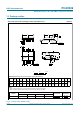
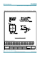
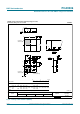
11.1 Bidirectional translation
For the bidirectional clamping configuration (higher voltage to lower voltage or lower
voltage to higher voltage), the EN input must be connected to VREF2 and both pins pulled
to HIGH side V
pu(D)
through a pull-up resistor (typically 200 k). This allows VREF2 to
regulate the EN input. A filter capacitor on VREF2 is recommended. The I
2
C-bus master
output can be totem pole or open-drain (pull-up resistors may be required) and the
I
2
C-bus device output can be totem pole or open-drain (pull-up resistors are required to
pull the SCL2 and SDA2 outputs to V
pu(D)
). However, if either output is totem pole, data
must be unidirectional or the outputs must be 3-stateable and be controlled by some
direction-control mechanism to prevent HIGH-to-LOW contentions in either direction. If
both outputs are open-drain, no direction control is needed.
The reference supply voltage (V
ref(1)
) is connected to the processor core power supply
voltage. When VREF2 is connected through a 200 k resistor to a 3.3 V to 5.5 V V
pu(D)
power supply, and V
ref(1)
is set between 1.0 V and (V
pu(D)
1 V), the output of each SCL1
and SDA1 has a maximum output voltage equal to VREF1, and the output of each SCL2
and SDA2 has a maximum output voltage equal to V
pu(D)
.
[1] All typical values are at T
amb
=25C.
11.2 How to size pull-up resistor value
Sizing the pull-up resistor on an open-drain bus is specific to the individual application and
is dependent on the following driver characteristics:
• The driver sink current
• The V
OL
of driver
• The V
IL
of the driver
• Frequency of operation
The following tables can be used to estimate the pull-up resistor value in different use
cases so that the minimum resistance for the pull-up resistor can be found.
Table 11
, Table 12 and Table 13 contain suggested minimum values of pull-up resistors for
the PCA9306 and NVT20xx devices with typical voltage translation levels and drive
currents. The calculated values assume that both drive currents are the same.
V
OL
=V
IL
=0.1 V
CC
and accounts for a 5%V
CC
tolerance of the supplies, 1%
resistor values. It should be noted that the resistor chosen in the final application should
be equal to or larger than the values shown in Table 11
, Table 12 and Table 13 to ensure
that the pass voltage is less than 10 % of the V
CC
voltage, and the external driver should
Table 10. Application operating conditions
Refer to Figure 11.
Symbol Parameter Conditions Min Typ
[1]
Max Unit
V
bias(ref)(2)
reference bias voltage (2) V
ref(1)
+0.6 2.1 5 V
V
I(EN)
input voltage on pin EN V
ref(1)
+0.6 2.1 5 V
V
ref(1)
reference voltage (1) 0 1.5 4.4 V
I
sw(pass)
pass switch current - 14 - mA
I
ref
reference current transistor - 5 - A
T
amb
ambient temperature operating in
free-air
40 - +85 C