
Datasheet


NXP Semiconductors
PCA9306
Dual bidirectional I
2
C-bus and SMBus voltage-level translator
© NXP B.V. 2014. All rights reserved.
For more information, please visit: http://www.nxp.com
For sales office addresses, please send an email to: salesaddresses@nxp.com
Date of release: 22 January 2014
Document identifier: PCA9306
Please be aware that important notices concerning this document and the product(s)
described herein, have been included in section ‘Legal information’.
19. Contents
1 General description. . . . . . . . . . . . . . . . . . . . . . 1
2 Features and benefits . . . . . . . . . . . . . . . . . . . . 2
3 Ordering information. . . . . . . . . . . . . . . . . . . . . 3
3.1 Ordering options. . . . . . . . . . . . . . . . . . . . . . . . 3
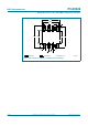
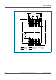
4 Functional diagram . . . . . . . . . . . . . . . . . . . . . . 4
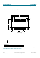
5 Pinning information. . . . . . . . . . . . . . . . . . . . . . 5
5.1 Pinning . . . . . . . . . . . . . . . . . . . . . . . . . . . . . . . 5
5.2 Pin description . . . . . . . . . . . . . . . . . . . . . . . . . 6
6 Functional description . . . . . . . . . . . . . . . . . . . 7
6.1 Function table. . . . . . . . . . . . . . . . . . . . . . . . . . 7
7 Limiting values. . . . . . . . . . . . . . . . . . . . . . . . . . 7
8 Recommended operating conditions. . . . . . . . 7
9 Static characteristics. . . . . . . . . . . . . . . . . . . . . 8
10 Dynamic characteristics . . . . . . . . . . . . . . . . . . 9
11 Application information. . . . . . . . . . . . . . . . . . 10
11.1 Bidirectional translation . . . . . . . . . . . . . . . . . 11
11.2 How to size pull-up resistor value. . . . . . . . . . 11
11.3 How to design for maximum frequency
operation. . . . . . . . . . . . . . . . . . . . . . . . . . . . . 13
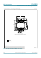
12 Package outline . . . . . . . . . . . . . . . . . . . . . . . . 15
13 Soldering of SMD packages . . . . . . . . . . . . . . 22
13.1 Introduction to soldering . . . . . . . . . . . . . . . . . 22
13.2 Wave and reflow soldering . . . . . . . . . . . . . . . 22
13.3 Wave soldering. . . . . . . . . . . . . . . . . . . . . . . . 22
13.4 Reflow soldering . . . . . . . . . . . . . . . . . . . . . . . 23
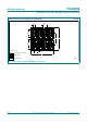
14 Soldering: PCB footprints. . . . . . . . . . . . . . . . 25
15 Abbreviations. . . . . . . . . . . . . . . . . . . . . . . . . . 32
16 Revision history. . . . . . . . . . . . . . . . . . . . . . . . 32
17 Legal information. . . . . . . . . . . . . . . . . . . . . . . 33
17.1 Data sheet status . . . . . . . . . . . . . . . . . . . . . . 33
17.2 Definitions. . . . . . . . . . . . . . . . . . . . . . . . . . . . 33
17.3 Disclaimers. . . . . . . . . . . . . . . . . . . . . . . . . . . 33
17.4 Trademarks. . . . . . . . . . . . . . . . . . . . . . . . . . . 34
18 Contact information. . . . . . . . . . . . . . . . . . . . . 34
19 Contents . . . . . . . . . . . . . . . . . . . . . . . . . . . . . . 35