
Datasheet


PCA9306 All information provided in this document is subject to legal disclaimers. © NXP B.V. 2014. All rights reserved.
Product data sheet Rev. 8 — 22 January 2014 6 of 35
NXP Semiconductors
PCA9306
Dual bidirectional I
2
C-bus and SMBus voltage-level translator
5.2 Pin description
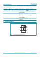
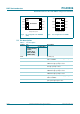
Fig 8. Pin configuration for XSON8U
(GD1)
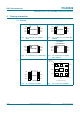
Fig 9. Pin configuration for XSON8
002aae014
Transparent top view
8
7
6
5
1
2
3
4
GND
VREF1
SCL1
SDA1
EN
VREF2
SCL2
SDA2
PCA9306GD1
002aaf393
4
3
2
1
5
6
7
8
PCA9306GF
Transparent top view
VREF1
GND
SCL1
VREF2
EN
SCL2
SDA1 SDA2
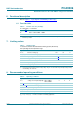
Table 3. Pin description
Symbol Pin Description
SO8,
TSSOP8 (MSOP8),
TSSOP8,
VSSOP8 (DC1),
XQFN8, XSON8,
XSON8U (GD1)
VSSOP8 (DC)
GND 1 4 ground (0 V)
VREF1 2 1 low-voltage side reference supply voltage for
SCL1 and SDA1
SCL1 3 2 serial clock, low-voltage side; connect to
VREF1 through a pull-up resistor
SDA1 4 3 serial data, low-voltage side; connect to VREF1
through a pull-up resistor
SDA2 5 5 serial data, high-voltage side; connect to
VREF2 through a pull-up resistor
SCL2 6 6 serial clock, high-voltage side; connect to
VREF2 through a pull-up resistor
VREF2 7 7 high-voltage side reference supply voltage for
SCL2 and SDA2
EN 8 8 switch enable input; connect to VREF2 and
pull-up through a high resistor