
Datasheet


PCA9306 All information provided in this document is subject to legal disclaimers. © NXP B.V. 2014. All rights reserved.
Product data sheet Rev. 8 — 22 January 2014 9 of 35
NXP Semiconductors
PCA9306
Dual bidirectional I
2
C-bus and SMBus voltage-level translator
10. Dynamic characteristics
Table 8. Dynamic characteristics (translating down)
T
amb
=
40
C to +85
C, unless otherwise specified. Values guaranteed by design.
Symbol Parameter Conditions C
L
=50pF C
L
=30pF C
L
=15pF Unit
Min Max Min Max Min Max
V
I(EN)
= 3.3 V; V
IH
=3.3V; V
IL
=0V; V
M
= 1.15 V (see Figure 10)
t
PLH
LOW to HIGH
propagation delay
from (input) SCL2 or SDA2
to (output) SCL1 or SDA1
02.001.200.6ns
t
PHL
HIGH to LOW
propagation delay
from (input) SCL2 or SDA2
to (output) SCL1 or SDA1
02.001.500.75ns
V
I(EN)
= 2.5 V; V
IH
=2.5V; V
IL
=0V; V
M
= 0.75 V (see Figure 10)
t
PLH
LOW to HIGH
propagation delay
from (input) SCL2 or SDA2
to (output) SCL1 or SDA1
02.001.200.6ns
t
PHL
HIGH to LOW
propagation delay
from (input) SCL2 or SDA2
to (output) SCL1 or SDA1
02.501.500.75ns
Table 9. Dynamic characteristics (translating up)
T
amb
=
40
C to +85
C, unless otherwise specified. Values guaranteed by design.
Symbol Parameter Conditions C
L
=50pF C
L
=30pF C
L
=15pF Unit
Min Max Min Max Min Max
V
I(EN)
= 3.3 V; V
IH
=2.3V; V
IL
=0V; V
TT
= 3.3 V; V
M
=1.15V; R
L
= 300 (see Figure 10)
t
PLH
LOW to HIGH
propagation delay
from (input) SCL1 or SDA1
to (output) SCL2 or SDA2
01.750 1.0 0 0.5ns
t
PHL
HIGH to LOW
propagation delay
from (input) SCL1 or SDA1
to (output) SCL2 or SDA2
02.7501.650 0.8ns
V
I(EN)
= 2.5 V; V
IH
=1.5V; V
IL
=0V; V
TT
= 2.5 V; V
M
=0.75V; R
L
= 300 (see Figure 10)
t
PLH
LOW to HIGH
propagation delay
from (input) SCL1 or SDA1
to (output) SCL2 or SDA2
01.750 1.0 0 0.5ns
t
PHL
HIGH to LOW
propagation delay
from (input) SCL1 or SDA1
to (output) SCL2 or SDA2
03.302.001.0ns
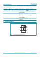
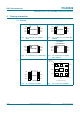
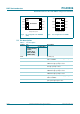
a. Load circuit b. Timing diagram
S1 = translating up; S2 = translating down.
C
L
includes probe and jig capacitance.
All input pulses are supplied by generators having the following characteristics: PRR 10 MHz; Z
o
=50; t
r
2ns; t
f
2ns.
The outputs are measured one at a time, with one transition per measurement.
Fig 10. Load circuit for outputs
002aab845
V
TT
R
L
S1
S2 (open)
C
L
from output under test
002aab846
V
IH
V
IL
V
M
V
M
input
output
V
OH
V
OL
V
M
V
M