
Datasheet

PCA9551_8 © NXP B.V. 2008. All rights reserved.
Product data sheet Rev. 08 — 31 July 2008 4 of 26
NXP Semiconductors
PCA9551
8-bit I
2
C-bus LED driver with programmable blink rates
[1] HVQFN16 package die supply ground is connected to both V
SS
pin and exposed center pad. V
SS
pin must
be connected to supply ground for proper device operation. For enhanced thermal, electrical, and board
level performance, the exposed pad needs to be soldered to the board using a corresponding thermal pad
on the board and for proper heat conduction through the board, thermal vias need to be incorporated in the
PCB in the thermal pad region.
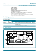
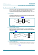
6. Functional description
Refer to Figure 1 “Block diagram of PCA9551”.
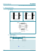
6.1 Device address
Following a START condition, the bus master must output the address of the slave it is
accessing. The address of the PCA9551 is shown in Figure 5. To conserve power, no
internal pull-up resistors are incorporated on the hardware selectable address pins and
they must be pulled HIGH or LOW.
The last bit of the address byte defines the operation to be performed. When set to logic 1
a read is selected, while a logic 0 selects a write operation.
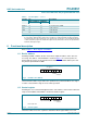
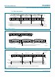
6.2 Control register
Following the successful acknowledgement of the slave address, the bus master will send
a byte to the PCA9551, which will be stored in the Control register.
The lowest 3 bits are used as a pointer to determine which register will be accessed.
LED7 12 10 LED driver 7
RESET 13 11 reset input (active LOW)
SCL 14 12 serial clock line
SDA 15 13 serial data line
V
DD
16 14 supply voltage
Table 2. Pin description
…continued
Symbol Pin Description
SO16, TSSOP16 HVQFN16
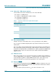
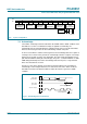
Fig 5. PCA9551 slave address
002aac505
1 1 0 0 A2 A1 A0 R/W
fixed
slave address
hardware
selectable
Reset state: 00h
Fig 6. Control register
002aac506
0 0 0 AI 0 B2 B1 B0
register address
Auto-Increment flag