
Datasheet

PCA9551_8 © NXP B.V. 2008. All rights reserved.
Product data sheet Rev. 08 — 31 July 2008 5 of 26
NXP Semiconductors
PCA9551
8-bit I
2
C-bus LED driver with programmable blink rates
If the Auto-Increment (AI) flag is set, the three low order bits of the Control register are
automatically incremented after a read or write. This allows the user to program the
registers sequentially. The contents of these bits will rollover to ‘000’ after the last register
is accessed.
When the Auto-Increment flag is set (AI = 1) and a read sequence is initiated, the
sequence must start by reading a register different from ‘0' (B2 B1 B0 ≠ 000).
Only the 3 least significant bits are affected by the AI flag. Unused bits must be
programmed with zeroes.
6.2.1 Control register definition
6.3 Register descriptions
6.3.1 INPUT - Input register
The INPUT register reflects the state of the device pins. Writes to this register will be
acknowledged but will have no effect.
Remark: The default value ‘X’ is determined by the externally applied logic level (normally
logic 1) when used for directly driving LED with pull-up to V
DD
.
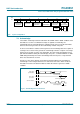
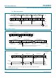
6.3.2 PSC0 - Frequency Prescaler 0
PSC0 is used to program the period of the PWM output.
The period of BLINK0 = (PSC0 + 1) / 38.
Remark: Prescaler calculation is different between the PCA9551 and other PCA955x
LED blinkers. A divider ratio of 38 instead of 44 is used. This different divider ratio causes
the blinking frequency to be 13 % (1 − 38 / 44) lower when the same 8-bit word is used.
The programmed value of Frequency Prescaler 0 must be adjusted to compensate for this
difference in applications where the PCA9551 is used in conjunction with other PCA955x
LED blinkers and the observed blinking frequencies need to be the same.
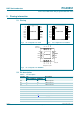
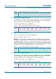
Table 3. Register summary
B2 B1 B0 Symbol Access Description
0 0 0 INPUT read only input register
0 0 1 PSC0 read/write frequency prescaler 0
0 1 0 PWM0 read/write PWM register 0
0 1 1 PSC1 read/write frequency prescaler 1
1 0 0 PWM1 read/write PWM register 1
1 0 1 LS0 read/write LED0 to LED3 selector
1 1 0 LS1 read/write LED4 to LED7 selector
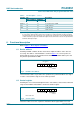
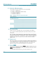
Table 4. INPUT - Input register description
Bit 7 6 5 4 3 2 1 0
Symbol LED7 LED6 LED5 LED4 LED3 LED2 LED1 LED0
Default XXXXXXXX