
Datasheet

PCA9551_8 © NXP B.V. 2008. All rights reserved.
Product data sheet Rev. 08 — 31 July 2008 7 of 26
NXP Semiconductors
PCA9551
8-bit I
2
C-bus LED driver with programmable blink rates
6.3.6 LS0 to LS1 - LED selector registers
The LSn LED select registers determine the source of the LED data.
00 = output is set LOW (LED on)
01 = output is set high-impedance (LED off; default)
10 = output blinks at PWM0 rate
11 = output blinks at PWM1 rate
6.4 Pins used as GPIOs
LED pins not used to control LEDs can be used as general purpose I/Os (GPIOs).
For use as input, set LEDn to high-impedance (01) and then read the pin state via the
Input register.
For use as output, connect external pull-up resistor to the pin and size it according to the
DC recommended operating characteristics. LEDn output pin is HIGH when the output is
programmed as high-impedance, and LOW when the output is programmed LOW through
the ‘LED selector’ register. The output can be pulse-width controlled when PWM0 or
PWM1 are used.
6.5 Power-on reset
When power is applied to V
DD
, an internal Power-On Reset (POR) holds the PCA9551 in
a reset condition until V
DD
has reached V
POR
. At that point, the reset condition is released
and the PCA9551 registers are initialized to their default states, all the outputs in the
OFF state. Thereafter, V
DD
must be lowered below 0.2 V to reset the device.
6.6 External RESET
A reset can be accomplished by holding the RESET pin LOW for a minimum of t
w(rst)
. The
PCA9551 registers and I
2
C-bus state machine will be held in their default states until the
RESET input is once again HIGH.
This input requires a pull-up resistor to V
DD
if no active connection is used.
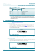
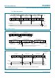
Table 9. LS0 to LS1 - LED selector registers bit description
Legend: * default value.
Register Bit Value Description
LS0 - LED0 to LED3 selector
LS0 7:6 01* LED3 selected
5:4 01* LED2 selected
3:2 01* LED1 selected
1:0 01* LED0 selected
LS1 - LED4 to LED7 selector
LS1 7:6 01* LED7 selected
5:4 01* LED6 selected
3:2 01* LED5 selected
1:0 01* LED4 selected