PCF2123 SPI Real time clock/calendar Rev. 6 — 15 July 2013 Product data sheet 1. General description The PCF2123 is a CMOS1 Real-Time Clock (RTC) and calendar optimized for low power applications. Data is transferred serially via a Serial Peripheral Interface (SPI-bus) with a maximum data rate of 6.25 Mbit/s. An alarm and timer function is also available providing the possibility to generate a wake-up signal on an interrupt pin. An offset register allows fine tuning of the clock. 2.
PCF2123 NXP Semiconductors SPI Real time clock/calendar 4. Ordering information Table 1. Ordering information Type number Package Name Description Version PCF2123BS HVQFN16 plastic thermal enhanced very thin quad flat package; no leads; 16 terminals; body 3 3 0.85 mm SOT758-1 PCF2123TS TSSOP14 plastic thin shrink small outline package; 14 leads; body width 4.
PCF2123 NXP Semiconductors SPI Real time clock/calendar 6. Block diagram OSCI CLKOE COSCI OSCILLATOR 32.
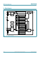
PCF2123 NXP Semiconductors SPI Real time clock/calendar 7. Pinning information OSCO 1 TEST 2 13 VDD 14 n.c. terminal 1 index area 15 n.c. 16 OSCI 7.1 Pinning 12 CLKOUT 11 CLKOE PCF2123BS 10 SCL 6 7 8 n.c. SDO 9 n.c. 4 5 CE 3 VSS INT SDI 001aai550 OSCI 1 14 VDD OSCO 2 13 CLKOUT n.c. 3 TEST 4 INT 5 10 SCL CE 6 9 SDI VSS 7 8 SDO 12 CLKOE PCF2123TS Transparent top view 001aai551 For mechanical details, see Figure 31 on page 45. Fig 2. 11 n.c. Top view.
PCF2123 NXP Semiconductors SPI Real time clock/calendar 7.2 Pin description Table 4. Pin description Symbol Pin Description HVQFN16 TSSOP14 PCF2123Ux (PCF2123BS/1) (PCF2123TS/1) (bare die) OSCI 16 1 7 oscillator input; high-impedance node; minimize wire length between quartz and package OSCO 1 2 8 oscillator output; high-impedance node; minimize wire length between quartz and package n.c.
PCF2123 NXP Semiconductors SPI Real time clock/calendar 8. Functional description The PCF2123 contains 16 8-bit registers with an auto-incrementing address counter, an on-chip 32.768 kHz oscillator with two integrated load capacitors, a frequency divider which provides the source clock for the Real Time Clock (RTC), a programmable clock output, and a 6.25 Mbit/s SPI-bus. An offset register allows fine tuning of the clock.
PCF2123 NXP Semiconductors SPI Real time clock/calendar 001aai558 250 IDD(1) (nA) 210 170 130 90 50 0 20 40 60 80 Rs(2) (kΩ) 100 Configuration: CLKOUT disabled, VDD = 3 V, timer clock set to 1⁄60 Hz. (1) IDD (nA) minimum power mode. (2) Maximum value for RS is 100 k. Fig 5. IDD with respect to quartz RS 8.1.2 Power consumptions with respect to timer mode Four source clocks are possible for the timer. The 4.096 kHz source clock will add the greatest part to the power consumption.
PCF2123 NXP Semiconductors SPI Real time clock/calendar 8.2 Register overview 16 registers are available. The time registers are encoded in the Binary Coded Decimal (BCD) format to simplify application use. Other registers are either bit-wise or standard binary. Table 5. Registers overview Bit positions labelled as - are not implemented and will return a 0 when read. The bit position labelled as -- is not implemented and will return a 0 or 1 when read.
PCF2123 NXP Semiconductors SPI Real time clock/calendar 8.3 Control registers 8.3.1 Register Control_1 Table 6. Bit 7 Control_1 - control and status register 1 (address 00h) bit description Symbol Value Description Reference EXT_TEST 0[1] normal mode Section 8.10 1 external clock test mode 6 N - unused - 5 STOP 0[1] the RTC source clock runs Section 8.11 1 the RTC clock is stopped; RTC divider chain flip-flops are asynchronously set to logic 0; CLKOUT at 32.768 kHz, 16.
PCF2123 NXP Semiconductors SPI Real time clock/calendar R/W b7 0 addr 00HEX b6 0 b5 0 b4 1 b3 0 b2 0 b1 0 software reset 58HEX b0 0 b7 0 b6 1 b5 0 b4 1 b3 1 b2 0 b1 0 b0 0 SCL CE (1) internal reset signal 001aai562 (1) When CE is inactive, the interface is reset. Fig 7. Software reset command After reset, the following mode is entered: • • • • • • 32.
PCF2123 NXP Semiconductors SPI Real time clock/calendar 8.3.2 Register Control_2 Table 8. Bit Control_2 - control and status register 2 (address 01h) bits description Symbol Value Description Reference 7 MI 0[1] minute interrupt is disabled Section 8.6.
PCF2123 NXP Semiconductors SPI Real time clock/calendar 8.4 Time and date function The majority of the registers are coded in the Binary Coded Decimal (BCD) format. BCD is used to simplify application use. An example is shown for the seconds in Table 10. 8.4.1 Register Seconds Table 9.
PCF2123 NXP Semiconductors SPI Real time clock/calendar OS = 1 and flag can not be cleared OS = 1 and flag can be cleared VDD oscillation OS flag OS flag cleared by software OS flag set when oscillation stops t oscillation now stable 001aai553 Fig 9. OS flag The oscillator may be stopped, for example, by grounding one of the oscillator pins, OSCI or OSCO. The oscillator is also considered to be stopped during the time between power-on and stable crystal resonance.
PCF2123 NXP Semiconductors SPI Real time clock/calendar 8.4.4 Register Days Table 13. Days - days register (address 05h) bit description Bit Symbol Value Place value Description 7 to 6 - - - unused 5 to 4 DAYS[1] 0 to 3 ten’s place actual day coded in BCD format 0 to 9 unit place 3 to 0 [1] The PCF2123 compensates for leap years by adding a 29th day to February if the year counter contains a value which is exactly divisible by 4, including the year 00. 8.4.
PCF2123 NXP Semiconductors SPI Real time clock/calendar Table 17. Month assignments in BCD format Month Upper-digit (ten’s place) Digit (unit place) Bit 4 Bit 3 Bit 2 Bit 1 Bit 0 January 0 0 0 0 1 February 0 0 0 1 0 March 0 0 0 1 1 April 0 0 1 0 0 May 0 0 1 0 1 June 0 0 1 1 0 July 0 0 1 1 1 August 0 1 0 0 0 September 0 1 0 0 1 October 1 0 0 0 0 November 1 0 0 0 1 December 1 0 0 1 0 8.4.7 Register Years Table 18.
PCF2123 NXP Semiconductors SPI Real time clock/calendar During read/write operations, the time counting circuits (memory locations 02h through 08h) are blocked. This prevents • Faulty reading of the clock and calendar during a carry condition • Incrementing the time registers during the read cycle After this read/write access is completed, the time circuit is released again and any pending request to increment the time counters that occurred during the read/write access is serviced.
PCF2123 NXP Semiconductors SPI Real time clock/calendar 8.5 Alarm function When one or more of these registers are loaded with a valid minute, hour, day, or weekday and its corresponding alarm enable bit (AE_x) is logic 0, then that information will be compared with the current minute, hour, day, and weekday. 8.5.1 Register Minute_alarm Table 19.
PCF2123 NXP Semiconductors SPI Real time clock/calendar 8.5.4 Register Weekday_alarm Table 22. Weekday_alarm - weekday alarm register (address 0Ch) bit description Bit Symbol Value Description 7 AE_W 0 weekday alarm is enabled 1[1] weekday alarm is disabled 6 to 3 - - unused 2 to 0 WEEKDAY_ALARM 0 to 6 weekday alarm information coded in BCD format [1] Default value. 8.5.
PCF2123 NXP Semiconductors SPI Real time clock/calendar The generation of interrupts from the alarm function is controlled via bit AIE (register Control_2, see Table 8). If bit AIE is enabled, the INT pin follows the condition of bit AF. AF will remain set until cleared by the interface. Once AF has been cleared, it will only be set again when the time increments to match the alarm condition once more. Alarm registers which have their AE_x bit logic 1 are ignored.
PCF2123 NXP Semiconductors SPI Real time clock/calendar 8.6 Timer functions The countdown timer has four selectable source clocks allowing for countdown periods in the range from 244 s to 4 h 15 min. There are also two pre-defined timers which can be used to generate an interrupt once per second or once per minute. For periods greater than 4 hours, the alarm function can be used. Registers 01h, 0Eh and 0Fh are used to control the timer function and output. 8.6.1 Register Timer_clkout Table 25.
PCF2123 NXP Semiconductors SPI Real time clock/calendar seconds counter 58 59 minutes counter 59 00 11 12 00 01 INT when SI enabled MSF when SI enabled INT when only MI enabled MSF when only MI enabled 001aaf905 In this example, TI_TP is set to logic 1 resulting in ⁄ Hz wide interrupt pulse and the MSF flag is not cleared after an interrupt. Fig 14. INT example for MI and SI Table 27.
PCF2123 NXP Semiconductors SPI Real time clock/calendar 8.6.4 Countdown timer function The 8-bit countdown timer at address 0Fh is controlled by the register Timer_clkout at address 0Eh. The register Timer_clkout selects one of 4 source clock frequencies for the timer (4.096 kHz, 64 Hz, 1 Hz, or 1⁄60 Hz) and enables or disables the timer. Table 29. Bits CTD0 and CTD1 for timer frequency selection and countdown timer durations CTD[1:0] Timer source clock frequency[1] Delay 00 4.096 kHz 244 s 62.
PCF2123 NXP Semiconductors SPI Real time clock/calendar therefore changing it without setting bit TE = 0 may result in a corrupted value loaded into the countdown counter which results in an undetermined countdown period for the first period. The countdown value n will, however, be correctly stored and correctly loaded on subsequent timer periods. When the countdown timer flag is set, an interrupt signal on INT will be generated provided that this mode is enabled. See Section 8.7.
PCF2123 NXP Semiconductors SPI Real time clock/calendar Three examples are given for clearing the flags. Clearing the flags is made by a write command, therefore bits 7, 6, 4, 1 and 0 must be written with their previous values. Repeatedly re-writing these bits has no influence on the functional behavior. Table 31.
PCF2123 NXP Semiconductors SPI Real time clock/calendar 8.7 Interrupt output An active LOW interrupt signal is available at pin INT. Operation is controlled via the bits of register Control_2. Interrupts may be sourced from four places: second and minute timer, countdown timer, alarm function or offset function. With bit TI_TP, the timer generated interrupts can be configured to either generate a pulse or to follow the status of the interrupt flags (bits TF and MSF).
PCF2123 NXP Semiconductors SPI Real time clock/calendar 8.7.1 Minute and second interrupts The pulse generator for the minute and second interrupt operates from an internal 64 Hz clock and consequently generates a pulse of 1⁄64 second in duration. If the MSF flag is cleared before the end of the INT pulse, then the INT pulse is shortened. This allows the source of a system interrupt to be cleared immediately it is serviced, i.e.
PCF2123 NXP Semiconductors SPI Real time clock/calendar countdown counter 01 n CDTF INT (1) SCL 8th clock instruction CLEAR INSTRUCTION 001aaf909 (1) Indicates normal duration of INT pulse (bit TI_TP = 1). Fig 18. Example of shortening the INT pulse by clearing the TF flag The timing shown for clearing bit TF in Figure 18 is also valid for the non-pulsed interrupt mode, i.e., when bit TI_TP = 0; INT may be shortened by setting bit TIE to logic 0. 8.7.
PCF2123 NXP Semiconductors SPI Real time clock/calendar 8.8 Clock output A programmable square wave is available at pin CLKOUT. Operation is controlled by the COF[2:0] bits in the register Timer_clkout. Frequencies of 32.768 kHz (default) down to 1 Hz can be generated for use as a system clock, microcontroller clock, input to a charge pump, or for calibration of the oscillator. Pin CLKOUT is an open-drain output and enabled at power-on. When disabled the output is high-impedance.
PCF2123 NXP Semiconductors SPI Real time clock/calendar 8.9 Offset register The PCF2123 incorporates an offset register (address 0Dh) which can be used to implement several functions, such as: • Ageing adjustment • Temperature compensation • Accuracy tuning The offset is made once every two hours in the normal mode, or once every hour in the course mode. Each LSB will introduce an offset of 2.17 ppm for normal mode and 4.34 ppm for course mode. The values of 2.17 ppm and 4.
PCF2123 NXP Semiconductors SPI Real time clock/calendar Table 39.
PCF2123 NXP Semiconductors SPI Real time clock/calendar Table 40. Effect of correction pulses Frequency (Hz) Effect of correction CLKOUT 32768 no effect 16384 no effect 8192 no effect 4096 no effect 2048 no effect 1024 no effect 1 affected Time source clock 4096 no effect 64 no effect 1 affected 1⁄ 60 affected 8.9.1 Offset calibration workflow The calibration offset has to be calculated based on the time.
PCF2123 NXP Semiconductors SPI Real time clock/calendar 8.10 External clock test mode A test mode is available which allows for on-board testing. In this mode it is possible to set up test conditions and control the operation of the RTC. The test mode is entered by setting bit EXT_TEST in register Control_1. Then pin CLKOUT becomes an input. The test mode replaces the internal clock signal with the signal applied to pin CLKOUT.
PCF2123 NXP Semiconductors SPI Real time clock/calendar 8.11 STOP bit function The function of the STOP bit is to allow for accurate starting of the time circuits. The STOP bit function will cause the upper part of the prescaler (F2 to F14) to be held in reset and thus no 1 Hz ticks will be generated. The time circuits can then be set and will not increment until the STOP bit is released (see Figure 22 and Table 41). The STOP bit function will not affect the output of 32.768 kHz, 16.384 kHz, or 8.
PCF2123 NXP Semiconductors SPI Real time clock/calendar Table 41. First increment of time circuits after STOP bit release Bit Prescaler bits[1] STOP F0F1-F2 to F14 1 Hz tick Time Comment hh:mm:ss Clock is running normally 0 12:45:12 01-0 0001 1101 0100 prescaler counting normally STOP bit is activated by user.
PCF2123 NXP Semiconductors SPI Real time clock/calendar 9. 3-line serial interface Data transfer to and from the device is made via a 3-wire SPI-bus (see Table 42). The data lines for input and output are split. The data input and output lines can be connected together to facilitate a bidirectional data bus. The chip enable signal is used to identify the transmitted data. Each data transfer is a byte, with the Most Significant Bit (MSB) sent first (see Figure 24). Table 42.
PCF2123 NXP Semiconductors SPI Real time clock/calendar Table 43. Command byte definition Bit Symbol 7 R/W Value Description data read or data write selection 0 write data 1 read data 6 to 4 SA 001 subaddress; other codes will cause the device to ignore data transfer 3 to 0 RA 0h to Fh register address range In Figure 25, the register Seconds is set to 45 seconds and the register Minutes is set to 10 minutes.
PCF2123 NXP Semiconductors SPI Real time clock/calendar In Figure 26, the Months and Years registers are read. In this example, pins SDI and SDO are not connected together. For this configuration, it is important that pin SDI is never left floating. It must always be driven either HIGH or LOW. If pin SDI is left open, high IDD currents may result. Short transition periods in the order of 200 ns will not cause any problems. 9.
PCF2123 NXP Semiconductors SPI Real time clock/calendar 10. Internal circuitry PCF2123 VDD OSCI CLKOE OSCO CLKOUT TEST SCL INT SDI CE SDO VSS 001aai552 Fig 28. Device diode protection diagram of PCF2123 11. Safety notes CAUTION This device is sensitive to ElectroStatic Discharge (ESD). Observe precautions for handling electrostatic sensitive devices. Such precautions are described in the ANSI/ESD S20.20, IEC/ST 61340-5, JESD625-A or equivalent standards. CAUTION Semiconductors are light sensitive.
PCF2123 NXP Semiconductors SPI Real time clock/calendar 12. Limiting values Table 44. Limiting values In accordance with the Absolute Maximum Rating System (IEC 60134). Symbol PCF2123 Product data sheet Parameter Conditions [1] Min Max Unit 0.5 +6.5 V VDD supply voltage IDD supply current 50 +50 mA VI input voltage [1] 0.5 +6.5 V VO output voltage [1] 0.5 +6.
PCF2123 NXP Semiconductors SPI Real time clock/calendar 13. Static characteristics Table 45. Static characteristics VDD = 1.1 V to 5.5 V; VSS = 0 V; Tamb = 40 C to +85 C; fosc = 32.768 kHz; quartz Rs = 15 k; CL = 7 pF; unless otherwise specified. Symbol Parameter Conditions Min Typ Max Unit supply voltage for clock data integrity; SPI-bus inactive 1.1 - 5.5 V Tamb = 25 C - 0.9 - V SPI-bus active 1.8 - 5.5 V fSCL = 4.5 MHz; VDD = 5 V - 250 400 A fSCL = 1.
PCF2123 NXP Semiconductors SPI Real time clock/calendar Table 45. Static characteristics …continued VDD = 1.1 V to 5.5 V; VSS = 0 V; Tamb = 40 C to +85 C; fosc = 32.768 kHz; quartz Rs = 15 k; CL = 7 pF; unless otherwise specified. Symbol Parameter Conditions Min Typ Max Unit Inputs VIL LOW-level input voltage - - 0.3VDD V VIH HIGH-level input voltage 0.7VDD - - V VI input voltage on pins CE, SDI, SCL, OSCI, CLKOE, CLKOUT 0.5 - +5.
PCF2123 NXP Semiconductors SPI Real time clock/calendar 14. Dynamic characteristics Table 46. SPI-bus characteristics VSS = 0 V; Tamb = 40 C to +85 C. All timing values are valid within the operating supply voltage and temperature range and referenced to VIL and VIH with an input voltage swing of VSS to VDD. Symbol Parameter Conditions VDD = 1.8 V VDD = 2.4 V VDD = 3.3 V VDD = 5.
PCF2123 NXP Semiconductors SPI Real time clock/calendar tw(CE) CE tsu(CE) tSCL tclk(H) tclk(L) tr tf trec(CE) th(CE) 80% SCL 20% WRITE tsu th SDI SDO R/W SA2 RA0 b6 b0 b7 b6 b0 Hi Z READ SDI b7 tt(SDI-SDO) tdis(SDO) td(R)SDO SDO Hi Z b7 b6 b0 001aai554 Fig 29. SPI-bus timing PCF2123 Product data sheet All information provided in this document is subject to legal disclaimers. Rev. 6 — 15 July 2013 © NXP B.V. 2013. All rights reserved.
PCF2123 NXP Semiconductors SPI Real time clock/calendar 15. Application information 1F supercapacitor 100 nF VDD CLKOE CLKOUT INT CE OSCI PCF2123 SCL OSCO VSS SDO SDI 001aai557 A 1 farad super capacitor combined with a low VF diode can be used as a standby or back-up supply. With the RTC in its minimum power configuration i.e. timer off and CLKOUT off, the RTC may operate for weeks. Fig 30.
PCF2123 NXP Semiconductors SPI Real time clock/calendar 16. Package outline HVQFN16: plastic thermal enhanced very thin quad flat package; no leads; 16 terminals; body 3 x 3 x 0.85 mm A B D SOT758-1 terminal 1 index area A E A1 c detail X e1 C 1/2 e e 5 y y1 C v M C A B w M C b 8 L 4 9 e e2 Eh 1/2 e 12 1 16 terminal 1 index area 13 Dh X 0 2.5 5 mm scale DIMENSIONS (mm are the original dimensions) UNIT A(1) max.
PCF2123 NXP Semiconductors SPI Real time clock/calendar TSSOP14: plastic thin shrink small outline package; 14 leads; body width 4.4 mm SOT402-1 E D A X c y HE v M A Z 8 14 Q (A 3) A2 A A1 pin 1 index θ Lp L 1 7 e detail X w M bp 0 2.5 5 mm scale DIMENSIONS (mm are the original dimensions) UNIT A max. A1 A2 A3 bp c D (1) E (2) e HE L Lp Q v w y Z (1) θ mm 1.1 0.15 0.05 0.95 0.80 0.25 0.30 0.19 0.2 0.1 5.1 4.9 4.5 4.3 0.65 6.6 6.2 1 0.75 0.50 0.
PCF2123 NXP Semiconductors SPI Real time clock/calendar 17. Bare die outline Wire bond die; 12 bonding pads PCF2123U/10 D A 6 7 5 8 9 10 11 12 P4 P3 4 x 0 E 3 0 y 2 P2 1 P1 X eD detail X 0 1 mm scale OUTLINE VERSION REFERENCES IEC JEDEC EUROPEAN PROJECTION JEITA ISSUE DATE 08-07-24 11-04-06 PCF2123U/10 Fig 33. Bare die outline PCF2123U/10 of PCF2123U/5GA/1 and PCF2123U/10AA/1 (for dimensions see Table 47) Table 47. Dimensions of PCF2123U/10 Original dimensions are in mm.
PCF2123 NXP Semiconductors SPI Real time clock/calendar WLCSP12: wafer level chip size package; 12 bumps. PCF2123U/12 D 6 7 PC2123-1 5 8 4 9 x0 10 E 0 y 3 2 11 e 12 1 Y e X P4 P3 A1 P2 A2 P1 A detail Y detail X 0 0.5 1 mm scale pcf2123u_12_do References Outline version IEC JEDEC JEITA PCF2123U/12 --- --- --- European projection Issue date 10-07-13 11-04-06 Fig 34.
PCF2123 NXP Semiconductors SPI Real time clock/calendar Table 48. Dimensions of PCF2123U/12 Original dimensions are in mm. Unit (mm) A[1] A1 A2[1] D[2] E[2] e P1[3] P2[4] P3[3] P4[4] PCF2123U/12AA max - 0.018 - - - 1.296 - 0.084 - 0.084 nom 0.22 0.015 0.2 1.492 1.449 - 0.09 0.081 0.09 0.081 min - 0.012 - - - 0.198 - 0.078 - 0.078 PCF2123U/12HA max - 0.018 - - - 1.296 - 0.084 - 0.084 nom 0.17 0.015 0.15 1.492 1.449 - 0.09 0.081 0.09 0.
PCF2123 NXP Semiconductors SPI Real time clock/calendar Table 50. Alignment mark dimension and location of all PCF2123U types Coordinates x y Location[1] 516.2 693 Dimension[2] 16 m 13 m [1] The x/y coordinates of the alignment mark location represent the position of the REF point (see Figure 35) with respect to the center (x/y = 0) of the chip; see Figure 33 and Figure 34.
PCF2123 NXP Semiconductors SPI Real time clock/calendar 18. Handling information All input and output pins are protected against ElectroStatic Discharge (ESD) under normal handling. When handling Metal-Oxide Semiconductor (MOS) devices ensure that all normal precautions are taken as described in JESD625-A, IEC 61340-5 or equivalent standards. 19. Packing information 1.492 mm (1) ~18 μm 1 1 1.
PCF2123 NXP Semiconductors SPI Real time clock/calendar PP PP PP PP PHWDO IUDPH VWUDLJKW HGJH RI WKH ZDIHU PP PP P P SODVWLF ILOP DDD Fig 37. Film Frame Carrier (FFC) for 6 inch wafer (PCF2123U/10AA/1) PP PP PP PP SODVWLN PP PHWDOO IUDPH VWUDLJKW HGJH RI WKH ZDIHU PP PP P P SODVWLF ILOP DDD Fig 38.
PCF2123 NXP Semiconductors SPI Real time clock/calendar 20. Soldering of SMD packages This text provides a very brief insight into a complex technology. A more in-depth account of soldering ICs can be found in Application Note AN10365 “Surface mount reflow soldering description”. 20.1 Introduction to soldering Soldering is one of the most common methods through which packages are attached to Printed Circuit Boards (PCBs), to form electrical circuits.
PCF2123 NXP Semiconductors SPI Real time clock/calendar 20.
PCF2123 NXP Semiconductors SPI Real time clock/calendar temperature maximum peak temperature = MSL limit, damage level minimum peak temperature = minimum soldering temperature peak temperature time 001aac844 MSL: Moisture Sensitivity Level Fig 39. Temperature profiles for large and small components For further information on temperature profiles, refer to Application Note AN10365 “Surface mount reflow soldering description”.
PCF2123 NXP Semiconductors SPI Real time clock/calendar 21. Footprint information for reflow soldering Footprint information for reflow soldering of HVQFN16 package SOT758-1 Hx Gx D P 0.025 0.025 C (0.105) SPx Hy SPy tot nSPx Gy SPy nSPy SLy By Ay SPx tot SLx Bx Ax solder land solder paste deposit solder land plus solder paste occupied area nSPx nSPy 2 2 Dimensions in mm P Ax Ay Bx By C D SLx SLy 0.50 4.00 4.00 2.20 2.20 0.90 0.24 1.50 1.
PCF2123 NXP Semiconductors SPI Real time clock/calendar Footprint information for reflow soldering of TSSOP14 package SOT402-1 Hx Gx P2 (0.125) (0.125) Hy By Gy Ay C D2 (4x) D1 P1 Generic footprint pattern Refer to the package outline drawing for actual layout solder land occupied area DIMENSIONS in mm P1 P2 Ay By C D1 D2 Gx Gy Hx Hy 0.650 0.750 7.200 4.500 1.350 0.400 0.600 4.950 5.300 5.800 7.450 sot402-1_fr Fig 41.
PCF2123 NXP Semiconductors SPI Real time clock/calendar 22. Abbreviations Table 54.
PCF2123 NXP Semiconductors SPI Real time clock/calendar 23.
PCF2123 NXP Semiconductors SPI Real time clock/calendar 25. Legal information 25.1 Data sheet status Document status[1][2] Product status[3] Definition Objective [short] data sheet Development This document contains data from the objective specification for product development. Preliminary [short] data sheet Qualification This document contains data from the preliminary specification. Product [short] data sheet Production This document contains the product specification.
PCF2123 NXP Semiconductors SPI Real time clock/calendar Export control — This document as well as the item(s) described herein may be subject to export control regulations. Export might require a prior authorization from competent authorities. Non-automotive qualified products — Unless this data sheet expressly states that this specific NXP Semiconductors product is automotive qualified, the product is not suitable for automotive use.
PCF2123 NXP Semiconductors SPI Real time clock/calendar 27. Tables Table 1. Table 2. Table 3. Table 4. Table 5. Table 6. Table 7. Table 8. Table 9. Table 10. Table 11. Table 12. Table 13. Table 14. Table 15. Table 16. Table 17. Table 18. Table 19. Table 20. Table 21. Table 22. Table 23. Table 24. Table 25. Table 26. Table 27. Table 28. Table 29. Table 30. Table 31. Table 32. Table 33. Table 34. Table 35. Table 36. Table 37. Ordering information . . . . . . . . . . . . . . . . . . . . .
PCF2123 NXP Semiconductors SPI Real time clock/calendar 28. Figures Fig 1. Fig 2. Fig 3. Fig 4. Fig 5. Fig 6. Fig 7. Fig 8. Fig 9. Fig 10. Fig 11. Fig 12. Fig 13. Fig 14. Fig 15. Fig 16. Fig 17. Fig 18. Fig 19. Fig 20. Fig 21. Fig 22. Fig 23. Fig 24. Fig 25. Fig 26. Fig 27. Fig 28. Fig 29. Fig 30. Fig 31. Fig 32. Fig 33. Fig 34. Fig 35. Fig 36. Fig 37. Fig 38. Fig 39. Fig 40. Fig 41. Block diagram of PCF2123 . . . . . . . . . . . . . . . . . .3 Pin configuration for HVQFN16 (PCF2123BS/1) . .
PCF2123 NXP Semiconductors SPI Real time clock/calendar 29. Contents 1 2 3 4 4.1 5 6 7 7.1 7.2 8 8.1 8.1.1 General description . . . . . . . . . . . . . . . . . . . . . . 1 Features and benefits . . . . . . . . . . . . . . . . . . . . 1 Applications . . . . . . . . . . . . . . . . . . . . . . . . . . . . 1 Ordering information . . . . . . . . . . . . . . . . . . . . . 2 Ordering options . . . . . . . . . . . . . . . . . . . . . . . . 2 Marking . . . . . . . . . . . . . . . . . . . . . . . . . . . . . .