
Datasheet

PCF85063A All information provided in this document is subject to legal disclaimers. © NXP Semiconductors N.V. 2014. All rights reserved.
Product data sheet Rev. 4 — 24 November 2014 34 of 65
NXP Semiconductors
PCF85063A
Tiny Real-Time Clock/calendar with alarm function and I
2
C-bus
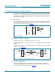
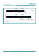
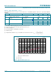
9.4 Acknowledge
The number of data bytes transferred between the START and STOP conditions from
transmitter to receiver is unlimited. Each byte of 8 bits is followed by an acknowledge
cycle.
• A slave receiver, which is addressed, must generate an acknowledge after the
reception of each byte
• Also a master receiver must generate an acknowledge after the reception of each
byte that has been clocked out of the slave transmitter
• The device that acknowledges must pull-down the SDA line during the acknowledge
clock pulse, so that the SDA line is stable LOW during the HIGH period of the
acknowledge related clock pulse (set-up and hold times must be considered)
• A master receiver must signal an end of data to the transmitter by not generating an
acknowledge on the last byte that has been clocked out of the slave. In this event, the
transmitter must leave the data line HIGH to enable the master to generate a STOP
condition
Acknowledgement on the I
2
C-bus is shown in Figure 21.
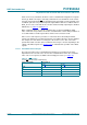
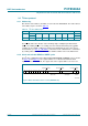
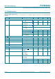
Fig 20. System configuration
PJD
6'$
6&/
0$67(5
75$160,77(5
5(&(,9(5
0$67(5
75$160,77(5
6/$9(
75$160,77(5
5(&(,9(5
6/$9(
5(&(,9(5
0$67(5
75$160,77(5
5(&(,9(5
Fig 21. Acknowledgement on the I
2
C-bus
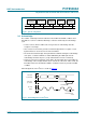
PEF
6
67$57
FRQGLWLRQ
FORFNSXOVHIRU
DFNQRZOHGJHPHQW
QRWDFNQRZOHGJH
DFNQRZOHGJH
GDWDRXWSXW
E\WUDQVPLWWHU
GDWDRXWSXW
E\UHFHLYHU
6&/IURP
PDVWHU