PCF8563 Real-time clock/calendar Rev. 10 — 3 April 2012 Product data sheet 1. General description The PCF8563 is a CMOS1 Real-Time Clock (RTC) and calendar optimized for low power consumption. A programmable clock output, interrupt output, and voltage-low detector are also provided. All addresses and data are transferred serially via a two-line bidirectional I2C-bus. Maximum bus speed is 400 kbit/s. The register address is incremented automatically after each written or read data byte. 2.
PCF8563 NXP Semiconductors Real-time clock/calendar 4. Ordering information Table 1. Ordering information Type number Package Name Description Version PCF8563BS/4 HVSON10 plastic thermal enhanced very thin small outline package; no leads; 10 terminals; body 3 3 0.85 mm SOT650-1 PCF8563P/F4 DIP8 plastic dual in-line package; 8 leads (300 mil) SOT97-1 PCF8563T/5 SO8 plastic small outline package; 8 leads; body width 3.
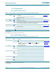
PCF8563 NXP Semiconductors Real-time clock/calendar 6. Block diagram OSCI OSCILLATOR 32.
PCF8563 NXP Semiconductors Real-time clock/calendar 7. Pinning information 7.1 Pinning terminal 1 index area OSCI 1 10 n.c. OSCO 2 9 VDD n.c. 3 8 CLKOUT INT 4 7 SCL VSS 5 6 SDA PCF8563BS OSCI 1 OSCO 2 Pin configuration for HVSON10 (PCF8563BS) OSCI 1 8 VDD OSCO 2 7 CLKOUT 3 6 SCL VSS 4 5 SDA INT 3 6 VSS 4 5 Top view. For mechanical details, see Figure 31. Fig 3.
PCF8563 NXP Semiconductors Real-time clock/calendar 7.2 Pin description Table 3. Pin description Symbol Pin DIP8, SO8, TSSOP8 HVSON10 OSCI 1 1 oscillator input OSCO 2 2 oscillator output INT 3 4 interrupt output (open-drain; active LOW) VSS 4 5[1] ground SDA 5 6 serial data input and output SCL 6 7 serial clock input CLKOUT 7 8 clock output, open-drain VDD 8 9 supply voltage n.c.
PCF8563 NXP Semiconductors Real-time clock/calendar 8. Functional description The PCF8563 contains sixteen 8-bit registers with an auto-incrementing register address, an on-chip 32.768 kHz oscillator with one integrated capacitor, a frequency divider which provides the source clock for the Real-Time Clock (RTC) and calender, a programmable clock output, a timer, an alarm, a voltage-low detector, and a 400 kHz I2C-bus interface.
PCF8563 NXP Semiconductors Real-time clock/calendar 8.2 Register organization Table 4. Formatted registers overview Bit positions labelled as x are not relevant. Bit positions labelled with N should always be written with logic 0; if read they could be either logic 0 or logic 1. After reset, all registers are set according to Table 27.
PCF8563 NXP Semiconductors Real-time clock/calendar 8.3 Control registers 8.3.1 Register Control_status_1 Table 5. Bit 7 Control_status_1 - control and status register 1 (address 00h) bit description Symbol Value Description Reference TEST1 0[1] normal mode Section 8.
PCF8563 NXP Semiconductors Real-time clock/calendar 8.3.2.1 Interrupt output Bits TF and AF: When an alarm occurs, AF is set to logic 1. Similarly, at the end of a timer countdown, TF is set to logic 1. These bits maintain their value until overwritten using the interface. If both timer and alarm interrupts are required in the application, the source of the interrupt can be determined by reading these bits.
PCF8563 NXP Semiconductors Real-time clock/calendar 8.4 Time and date registers The majority of the registers are coded in the BCD format to simplify application use. 8.4.1 Register VL_seconds Table 8.
PCF8563 NXP Semiconductors Real-time clock/calendar The VL flag is intended to detect the situation when VDD is decreasing slowly, for example under battery operation. Should the oscillator stop or VDD reach Vlow before power is re-asserted, then the VL flag is set. This will indicate that the time may be corrupted. 8.4.2 Register Minutes Table 10.
PCF8563 NXP Semiconductors Real-time clock/calendar Table 14. Weekday assignments Day[1] Bit 2 1 0 Sunday 0 0 0 Monday 0 0 1 Tuesday 0 1 0 Wednesday 0 1 1 Thursday 1 0 0 Friday 1 0 1 Saturday 1 1 0 [1] Definition may be re-assigned by the user. 8.4.6 Register Century_months Table 15.
PCF8563 NXP Semiconductors Real-time clock/calendar 8.4.7 Register Years Table 17. Bit Years - years register (08h) bit description Symbol Value Place value Description 7 to 4 YEARS 0 to 9 ten’s place 3 to 0 0 to 9 unit place [1] actual year coded in BCD format[1] When the register Years overflows from 99 to 00, the century bit C in the register Century_months is toggled. 8.5 Setting and reading the time Figure 8 shows the data flow and data dependencies starting from the 1 Hz clock tick.
PCF8563 NXP Semiconductors Real-time clock/calendar t<1s START SLAVE ADDRESS DATA DATA STOP 013aaa215 Fig 9. Access time for read/write operations As a consequence of this method, it is very important to make a read or write access in one go, that is, setting or reading seconds through to years should be made in one single access. Failing to comply with this method could result in the time becoming corrupted.
PCF8563 NXP Semiconductors Real-time clock/calendar 8.6 Alarm registers 8.6.1 Register Minute_alarm Table 18. Minute_alarm - minute alarm register (address 09h) bit description Bit Symbol Value Place value Description 7 AE_M 0 - minute alarm is enabled 1[1] - minute alarm is disabled 6 to 4 MINUTE_ALARM 0 to 5 ten’s place 3 to 0 0 to 9 unit place minute alarm information coded in BCD format [1] Default value. 8.6.2 Register Hour_alarm Table 19.
PCF8563 NXP Semiconductors Real-time clock/calendar 8.6.5 Alarm flag By clearing the alarm enable bit (AE_x) of one or more of the alarm registers, the corresponding alarm condition(s) are active. When an alarm occurs, AF is set to logic 1. The asserted AF can be used to generate an interrupt (INT). The AF is cleared using the interface. The registers at addresses 09h through 0Ch contain alarm information.
PCF8563 NXP Semiconductors Real-time clock/calendar 8.7 Register CLKOUT_control and clock output Frequencies of 32.768 kHz (default), 1.024 kHz, 32 Hz, and 1 Hz can be generated for use as a system clock, microcontroller clock, input to a charge pump, or for calibration of the oscillator. Table 22.
PCF8563 NXP Semiconductors Real-time clock/calendar 8.8.2 Register Timer Table 24. Timer - timer value register (address 0Fh) bit description Bit Symbol Value Description 7 to 0 TIMER[7:0] 00h to FFh countdown period in seconds: n CountdownPeriod = -------------------------------------------------------------SourceClockFrequency where n is the countdown value Table 25.
PCF8563 NXP Semiconductors Real-time clock/calendar 8.9 EXT_CLK test mode A test mode is available which allows for on-board testing. In such a mode it is possible to set up test conditions and control the operation of the RTC. The test mode is entered by setting bit TEST1 in register Control_status_1. Then pin CLKOUT becomes an input. The test mode replaces the internal 64 Hz signal with the signal applied to pin CLKOUT.
PCF8563 NXP Semiconductors Real-time clock/calendar 8.10 STOP bit function The function of the STOP bit is to allow for accurate starting of the time circuits. The STOP bit function will cause the upper part of the prescaler (F2 to F14) to be held in reset and thus no 1 Hz ticks will be generated (see Figure 11). The time circuits can then be set and will not increment until the STOP bit is released (see Figure 12 and Table 26).
PCF8563 NXP Semiconductors Real-time clock/calendar Table 26. First increment of time circuits after STOP bit release Bit Prescaler bits STOP F0F1-F2 to F14 [1] 1 Hz tick Time Comment hh:mm:ss Clock is running normally 0 12:45:12 01-0 0001 1101 0100 prescaler counting normally STOP bit is activated by user.
PCF8563 NXP Semiconductors Real-time clock/calendar 8.11 Reset The PCF8563 includes an internal reset circuit which is active whenever the oscillator is stopped. In the reset state the I2C-bus logic is initialized including the address pointer and all registers are set according to Table 27. I2C-bus communication is not possible during reset. Table 27.
PCF8563 NXP Semiconductors Real-time clock/calendar 500 ns 2000 ns SDA SCL 8 ms power-on override active mgm664 Fig 13. POR override sequence PCF8563 Product data sheet All information provided in this document is subject to legal disclaimers. Rev. 10 — 3 April 2012 © NXP B.V. 2012. All rights reserved.
PCF8563 NXP Semiconductors Real-time clock/calendar 9. Characteristics of the I2C-bus The I2C-bus is for bidirectional, two-line communication between different ICs or modules. The two lines are a Serial DAta line (SDA) and a Serial CLock line (SCL). Both lines must be connected to a positive supply via a pull-up resistor. Data transfer may be initiated only when the bus is not busy. 9.1 Bit transfer One data bit is transferred during each clock pulse.
PCF8563 NXP Semiconductors Real-time clock/calendar SDA SCL MASTER TRANSMITTER RECEIVER SLAVE TRANSMITTER RECEIVER SLAVE RECEIVER MASTER TRANSMITTER RECEIVER MASTER TRANSMITTER mba605 Fig 16. System configuration 9.4 Acknowledge The number of data bytes transferred between the START and STOP conditions from transmitter to receiver is unlimited. Each byte of eight bits is followed by an acknowledge cycle.
PCF8563 NXP Semiconductors Real-time clock/calendar 9.5 I2C-bus protocol 9.5.1 Addressing Before any data is transmitted on the I2C-bus, the device which should respond is addressed first. The addressing is always carried out with the first byte transmitted after the start procedure. The PCF8563 acts as a slave receiver or slave transmitter. Therefore the clock signal SCL is only an input signal, but the data signal SDA is a bidirectional line.
PCF8563 NXP Semiconductors Real-time clock/calendar acknowledgement from slave S SLAVE ADDRESS 0 A acknowledgement from slave REGISTER ADDRESS A S acknowledgement from slave SLAVE ADDRESS 1 A DATA A n bytes R/W R/W acknowledgement from master auto increment memory register address (1) no acknowledgement from master 1 DATA P last byte auto increment memory register address 013aaa041 (1) At this moment master transmitter becomes master receiver and PCF8563 slave receiver becomes slav
PCF8563 NXP Semiconductors Real-time clock/calendar 9.6 Interface watchdog timer t<1s data START SLAVE ADDRESS WD timer DATA DATA STOP WD timer tracking time counters running time counters frozen running 013aaa420 a. Correct data transfer: read or write 1s
PCF8563 NXP Semiconductors Real-time clock/calendar 10. Internal circuitry VDD OSCI CLKOUT OSCO SCL INT VSS SDA PCF8563 013aaa348 Fig 23. Device diode protection diagram PCF8563 Product data sheet All information provided in this document is subject to legal disclaimers. Rev. 10 — 3 April 2012 © NXP B.V. 2012. All rights reserved.
PCF8563 NXP Semiconductors Real-time clock/calendar 11. Limiting values Table 28. Limiting values In accordance with the Absolute Maximum Rating System (IEC 60134). Symbol Parameter Conditions Min Max Unit VDD supply voltage 0.5 +6.5 V IDD supply current 50 +50 mA VI input voltage on pins SCL, SDA, and OSCI 0.5 +6.5 V VO output voltage on pins CLKOUT and INT 0.5 +6.
PCF8563 NXP Semiconductors Real-time clock/calendar 12. Static characteristics Table 29. Static characteristics VDD = 1.8 V to 5.5 V; VSS = 0 V; Tamb = 40 C to +85 C; fosc = 32.768 kHz; quartz Rs = 40 k; CL = 8 pF; unless otherwise specified. Symbol Parameter Conditions Min Typ Max Unit supply voltage interface inactive; fSCL = 0 Hz; Tamb = 25 C [1] 1.0 - 5.5 V interface active; fSCL = 400 kHz [1] 1.8 - 5.5 V Vlow - 5.5 V - - 800 A - - 200 A VDD = 5.
PCF8563 NXP Semiconductors Real-time clock/calendar Table 29. Static characteristics …continued VDD = 1.8 V to 5.5 V; VSS = 0 V; Tamb = 40 C to +85 C; fosc = 32.768 kHz; quartz Rs = 40 k; CL = 8 pF; unless otherwise specified. Symbol Parameter Conditions LOW-level output current output sink current; VOL = 0.
PCF8563 NXP Semiconductors Real-time clock/calendar mgr891 mgr890 1 IDD (μA) 4 frequency deviation (ppm) 2 0.8 0.6 0 0.4 −2 0.2 −4 0 −40 0 40 80 T (°C) Fig 26. Supply current IDD as a function of temperature T; CLKOUT = 32 kHz Product data sheet 0 2 4 VDD (V) 6 Tamb = 25 C; normalized to VDD = 3 V. VDD = 3 V; Timer = 1 minute. PCF8563 120 Fig 27. Frequency deviation as a function of supply voltage VDD All information provided in this document is subject to legal disclaimers. Rev.
PCF8563 NXP Semiconductors Real-time clock/calendar 13. Dynamic characteristics Table 30. Dynamic characteristics VDD = 1.8 V to 5.5 V; VSS = 0 V; Tamb = 40 C to +85 C; fosc = 32.768 kHz; quartz Rs = 40 k; CL = 8 pF; unless otherwise specified. Symbol Parameter Conditions Min Typ Max Unit 15 25 35 pF - 0.2 - ppm - - 100 k 7 - 12.
PCF8563 NXP Semiconductors Real-time clock/calendar SDA tBUF tLOW tf SCL tHD;STA tr tHD;DAT tHIGH tSU;DAT SDA tSU;STA tSU;STO mga728 Fig 28. I2C-bus timing waveforms PCF8563 Product data sheet All information provided in this document is subject to legal disclaimers. Rev. 10 — 3 April 2012 © NXP B.V. 2012. All rights reserved.
PCF8563 NXP Semiconductors Real-time clock/calendar 14. Application information VDD SDA SCL 1F MASTER TRANSMITTER/ RECEIVER 100 nF VDD SCL CLOCK CALENDAR OSCI PCF8563 OSCO VSS SDA VDD R SDA SCL (I2C-bus) R R: pull-up resistor tr R= Cb mgm665 Fig 29. Application diagram 14.1 Quartz frequency adjustment 14.1.1 Method 1: fixed OSCI capacitor By evaluating the average capacitance necessary for the application layout, a fixed capacitor can be used. The frequency is best measured via the 32.
PCF8563 NXP Semiconductors Real-time clock/calendar 15. Package outline HVSON10: plastic thermal enhanced very thin small outline package; no leads; 10 terminals; body 3 x 3 x 0.85 mm SOT650-1 0 1 2 mm scale X A B D A A1 E c detail X terminal 1 index area C e1 terminal 1 index area e 5 y y1 C v M C A B w M C b 1 L Eh 6 10 Dh DIMENSIONS (mm are the original dimensions) UNIT A(1) max. A1 b c D(1) Dh E(1) Eh e e1 L v w y y1 mm 1 0.05 0.00 0.30 0.18 0.2 3.1 2.
PCF8563 NXP Semiconductors Real-time clock/calendar DIP8: plastic dual in-line package; 8 leads (300 mil) SOT97-1 ME seating plane D A2 A A1 L c Z w M b1 e (e 1) b MH b2 5 8 pin 1 index E 1 4 0 5 10 mm scale DIMENSIONS (inch dimensions are derived from the original mm dimensions) UNIT A max. A1 min. A2 max. b b1 b2 c D (1) E (1) e e1 L ME MH w Z (1) max. mm 4.2 0.51 3.2 1.73 1.14 0.53 0.38 1.07 0.89 0.36 0.23 9.8 9.2 6.48 6.20 2.54 7.62 3.60 3.05 8.
PCF8563 NXP Semiconductors Real-time clock/calendar SO8: plastic small outline package; 8 leads; body width 3.9 mm SOT96-1 D E A X c y HE v M A Z 5 8 Q A2 A (A 3) A1 pin 1 index θ Lp 1 L 4 e detail X w M bp 0 2.5 5 mm scale DIMENSIONS (inch dimensions are derived from the original mm dimensions) UNIT A max. A1 A2 A3 bp c D (1) E (2) e HE L Lp Q v w y Z (1) mm 1.75 0.25 0.10 1.45 1.25 0.25 0.49 0.36 0.25 0.19 5.0 4.8 4.0 3.8 1.27 6.2 5.8 1.05 1.0 0.
PCF8563 NXP Semiconductors Real-time clock/calendar TSSOP8: plastic thin shrink small outline package; 8 leads; body width 3 mm D E SOT505-1 A X c y HE v M A Z 5 8 A2 pin 1 index (A3) A1 A θ Lp L 1 4 detail X e w M bp 0 2.5 5 mm scale DIMENSIONS (mm are the original dimensions) UNIT A max. A1 A2 A3 bp c D(1) E(2) e HE L Lp v w y Z(1) θ mm 1.1 0.15 0.05 0.95 0.80 0.25 0.45 0.25 0.28 0.15 3.1 2.9 3.1 2.9 0.65 5.1 4.7 0.94 0.7 0.4 0.1 0.1 0.1 0.70 0.
PCF8563 NXP Semiconductors Real-time clock/calendar 16. Handling information All input and output pins are protected against ElectroStatic Discharge (ESD) under normal handling. When handling Metal-Oxide Semiconductor (MOS) devices ensure that all normal precautions are taken as described in JESD625-A, IEC 61340-5 or equivalent standards. 17. Soldering of SMD packages This text provides a very brief insight into a complex technology.
PCF8563 NXP Semiconductors Real-time clock/calendar 17.3 Wave soldering Key characteristics in wave soldering are: • Process issues, such as application of adhesive and flux, clinching of leads, board transport, the solder wave parameters, and the time during which components are exposed to the wave • Solder bath specifications, including temperature and impurities 17.
PCF8563 NXP Semiconductors Real-time clock/calendar maximum peak temperature = MSL limit, damage level temperature minimum peak temperature = minimum soldering temperature peak temperature time 001aac844 MSL: Moisture Sensitivity Level Fig 34. Temperature profiles for large and small components For further information on temperature profiles, refer to Application Note AN10365 “Surface mount reflow soldering description”. 18. Abbreviations Table 33.
PCF8563 NXP Semiconductors Real-time clock/calendar 19.
PCF8563 NXP Semiconductors Real-time clock/calendar 20. Revision history Table 34. Revision history Document ID Release date Data sheet status Change notice Supersedes PCF8563 v.10 20120403 Product data sheet - PCF8563 v.9 - PCF8563 v.8 Modifications: PCF8563 v.9 • • Adjusted marking codes Adjusted text for FE = 0 in Table 22 20110616 Product data sheet PCF8563 v.8 20101118 Product data sheet - PCF8563 v.7 PCF8563 v.
PCF8563 NXP Semiconductors Real-time clock/calendar 21. Legal information 21.1 Data sheet status Document status[1][2] Product status[3] Objective [short] data sheet Development This document contains data from the objective specification for product development. Preliminary [short] data sheet Qualification This document contains data from the preliminary specification. Product [short] data sheet Production This document contains the product specification.
PCF8563 NXP Semiconductors Real-time clock/calendar Export control — This document as well as the item(s) described herein may be subject to export control regulations. Export might require a prior authorization from competent authorities. Non-automotive qualified products — Unless this data sheet expressly states that this specific NXP Semiconductors product is automotive qualified, the product is not suitable for automotive use.
PCF8563 NXP Semiconductors Real-time clock/calendar 23. Tables Table 1. Table 2. Table 3. Table 4. Table 5. Table 6. Table 7. Table 8. Table 9. Table 10. Table 11. Table 12. Table 13. Table 14. Table 15. Table 16. Table 17. Table 18. Table 19. Table 20. Table 21. Table 22. Table 23. Table 24. Table 25. Table 26. Table 27. Table 28. Table 29. Table 30. Table 31. Table 32. Table 33. Table 34. Ordering information . . . . . . . . . . . . . . . . . . . . .2 Marking codes . . . . . . . . . . . . . . . . . .
PCF8563 NXP Semiconductors Real-time clock/calendar 24. Figures Fig 1. Fig 2. Fig 3. Fig 4. Fig 5. Fig 6. Fig 7. Fig 8. Fig 9. Fig 10. Fig 11. Fig 12. Fig 13. Fig 14. Fig 15. Fig 16. Fig 17. Fig 18. Fig 19. Fig 20. Fig 21. Fig 22. Fig 23. Fig 24. Fig 25. Fig 26. Fig 27. Fig 28. Fig 29. Fig 30. Fig 31. Fig 32. Fig 33. Fig 34. Block diagram of PCF8563 . . . . . . . . . . . . . . . . . .3 Pin configuration for HVSON10 (PCF8563BS) . . .4 Pin configuration for DIP8 (PCF8563P) . . . . . . . . .
PCF8563 NXP Semiconductors Real-time clock/calendar 25. Contents 1 2 3 4 5 6 7 7.1 7.2 8 8.1 8.2 8.3 8.3.1 8.3.2 8.3.2.1 8.4 8.4.1 8.4.1.1 8.4.2 8.4.3 8.4.4 8.4.5 8.4.6 8.4.7 8.5 8.6 8.6.1 8.6.2 8.6.3 8.6.4 8.6.5 8.7 8.8 8.8.1 8.8.2 8.9 8.9.1 8.10 8.11 8.11.1 9 9.1 9.2 9.3 9.4 General description . . . . . . . . . . . . . . . . . . . . . . 1 Features and benefits . . . . . . . . . . . . . . . . . . . . 1 Applications . . . . . . . . . . . . . . . . . . . . . . . . . . . . 1 Ordering information . . . .