
Datasheet

Philips Semiconductors
PCF8594C-2
512 × 8-bit CMOS EEPROM with I
2
C-bus interface
Product data Rev. 05 — 25 October 2004 11 of 21
9397 750 14221
© Koninklijke Philips Electronics N.V. 2004. All rights reserved.
11. I
2
C-bus characteristics
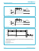
[1] The hold time required (not greater than 300 ns) to bridge the undefined region of the falling edge of SCL must be internally provided by
a transmitter.
SDA input/output (pin 5)
V
IL
LOW level input voltage −0.8 - 0.3V
DD
V
V
IH
HIGH level input voltage 0.7V
DD
- +6.5 V
V
OL
LOW level output voltage I
OL
= 3 mA; V
DD(min)
- - 0.4 V
I
LO
output leakage current V
OH
=V
DD
--1 µA
C
i
input capacitance V
I
=V
SS
--7 pF
Data retention time
t
S
data retention time T
amb
=55°C10−− years
Table 7: Characteristics
…continued
V
DD
= 2.5 V to 6.0 V; V
SS
=0V; T
amb
=
−
40
°
C to +85
°
C; unless otherwise specified.
Symbol Parameter Conditions Min Typ Max Unit
Table 8: I
2
C-bus characteristics
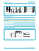
All of the timing values are valid within the operating supply voltage and ambient temperature range and refer to V
IL
and V
IH
with an input voltage swing from V
SS
to V
DD
; see Figure 9.
Symbol Parameter Conditions Min Max Unit
f
SCL
clock frequency 0 100 kHz
t
BUF
bus free time between a STOP and
START condition
4.7 −µs
t
HD;STA
START condition hold time after
which first clock pulse is generated
4.0 −µs
t
LOW
LOW level clock period 4.7 −µs
t
HIGH
HIGH level clock period 4.0 −µs
t
SU;STA
set-up time for START condition repeated start 4.7 −µs
t
HD;DAT
data hold time
for bus compatible masters 5 −µs
for bus devices
[1]
0 − ns
t
SU;DAT
data set-up time 250 − ns
t
r
SDA and SCL rise time − 1 µs
t
f
SDA and SCL fall time − 300 ns
t
SU;STO
set-up time for STOP condition 4.0 −µs