Freescale Semiconductor MC9S08SG32 DataSheet Addendum by: Microcontroller Solutions Group This is the MC9S08SG32 DataSheet set consisting of the following files: • MC9S08SG32 DataSheet Addendum, Rev 1 • MC9S08SG32 DataSheet, Rev 8 © Freescale Semiconductor, Inc., 2012. All rights reserved. MC9S08SG32 Rev. 8.
Freescale Semiconductor Addendum MC9S08SG32AD Rev. 1, 02/2012 MC9S08SG32 Data Sheet Addendum by: Microcontroller Solutions Group This errata document describes updates to the MC9S08SG32 Data Sheet, order number MC9S08SG32. For convenience, the addenda items are grouped by revision. Please check our website at http://www.freescale.com for the latest updates. © Freescale Semiconductor, Inc., 2012. All rights reserved. Table of Contents 1 2 Addendum for Revision 8.0. . . . . . . . . . . . . . . . . .
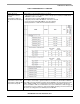
Addendum for Revision 8.0 1 Addendum for Revision 8.0 Table 1. MC9S08SG32 Rev. 1 Addendum Location Description Chapter “Memory”/ Section In Figure 4-1. MC9S08SG32/MC9S08SG16 Memory Map for device MC9S08SG16 change the “MC9S08SG32 Series value of “Unimplemented Bytes” from “26,538” to “26,528”. Memory Map”/Figure 4-1.
Addendum for Revision 8.0 Table 1. MC9S08SG32 Rev. 1 Addendum Location Description Chapter “Electrical Update Table A-3. Thermal Characteristics as follows: Characteristics”/Section • —Change the value for row “Thermal resistance,Single-layer board/28-pin TSSOP/Airflow “Thermal @200ft/min.” from 71 to 72 C/W Characteristics”/Table A-3. —Change the value for 16-pin TSSOP/Thermalresistance Thermal Characteristics/Page 1.Single layer board / Airflow @ 200ft/min. from 108 to 113 C/W. 293 2.
Revision History Table 1. MC9S08SG32 Rev. 1 Addendum Location Description Chapter “Electrical Characteristics”/Section “Flash Specifications”/Table “A-16. Flash Characteristics”/Page 323 2 In Table A-16 Flash Characteristics/row 9/column "Characteristic", change the temperature parameter names as follows: Standard: -40oC to +125oC HT: -40oC to +150oC T = 25oC Revision History Table 2 provides a revision history for this document. Table 2. Revision History Table Rev. Number 1.
How to Reach Us: Home Page: www.freescale.com Web Support: http://www.freescale.com/support USA/Europe or Locations Not Listed: Freescale Semiconductor, Inc. Technical Information Center, EL516 2100 East Elliot Road Tempe, Arizona 85284 +1-800-521-6274 or +1-480-768-2130 www.freescale.
MC9S08SG32 MC9S08SG16 Data Sheet Now Includes High-Temperature (up to 150 °C) Devices! HCS08 Microcontrollers MC9S08SG32 Rev. 8 5/2010 freescale.
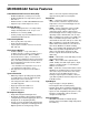
MC9S08SG32 Series Features 8-Bit HCS08 Central Processor Unit (CPU) • 40-MHz HCS08 CPU (central processor unit) • 36-MHz HCS08 CPU for temperatures greater than 125 °C • HC08 instruction set with added BGND instruction • Support for up to 32 interrupt/reset sources On-Chip Memory • FLASH read/program/erase over full operating voltage and temperature from –40 up to 150 °C • Random-access memory (RAM) • Security circuitry to prevent unauthorized access to RAM and FLASH contents Power-Saving Modes • Two very
MC9S08SG32 Data Sheet Covers MC9S08SG32 MC9S08SG16 MC9S08SG32 Rev. 8 5/2010 Freescale™ and the Freescale logo are trademarks of Freescale Semiconductor, Inc. © Freescale Semiconductor, Inc., 2007-2010. All rights reserved.
Revision History To provide the most up-to-date information, the revision of our documents on the World Wide Web will be the most current. Your printed copy may be an earlier revision. To verify you have the latest information available, refer to: http://freescale.com/ The following revision history table summarizes changes contained in this document.
Revision Number 8 Revision Date 5/2010 Description of Changes • In the A.9 ICS Characteristic table, changed row 9 parameter classification from a D to a P to indicate that these parameters are guaranteed during production testing on each individual device. • In the A.16 Flash Charateristic table, added the AEC temperature range to row 9. • Revised Figure 2-1 so that the RESET pin shows the overbar. © Freescale Semiconductor, Inc., 2007-2010. All rights reserved.
MC9S08SG32 Data Sheet, Rev.
Contents Section Number Title Page Chapter 1 Device Overview ...................................................................... 21 Chapter 2 Pins and Connections ............................................................. 25 Chapter 3 Modes of Operation ................................................................. 33 Chapter 4 Memory ..................................................................................... 39 Chapter 5 Resets, Interrupts, and General System Control.........
Contents Section Number Title Page Chapter 1 Device Overview 1.1 1.2 1.3 Devices in the MC9S08SG32 Series............................................................................................... 21 MCU Block Diagram ...................................................................................................................... 22 System Clock Distribution ..............................................................................................................
Section Number 4.6 4.7 Title Page 4.5.4 Burst Program Execution.................................................................................................. 51 4.5.5 Access Errors .................................................................................................................... 53 4.5.6 FLASH Block Protection.................................................................................................. 53 4.5.7 Vector Redirection ................................................
Section Number 6.5 6.6 Title Page 6.4.2 Edge and Level Sensitivity................................................................................................ 81 6.4.3 Pull-up/Pull-down Resistors ............................................................................................. 81 6.4.4 Pin Interrupt Initialization................................................................................................. 81 Pin Behavior in Stop Modes..................................................
Section Number 8.5 8.6 8.7 Title Page External Signal Description .......................................................................................................... 119 Memory Map ................................................................................................................................ 119 8.6.1 Register Descriptions ...................................................................................................... 119 Functional Description ..............................
Section Number 9.6 Title Page 9.5.1 ADC Module Initialization Example ............................................................................. 144 Application Information................................................................................................................ 146 9.6.1 External Pins and Routing .............................................................................................. 146 9.6.2 Sources of Error ...............................................................
Section Number Title Page 11.3.1 ICS Control Register 1 (ICSC1) ..................................................................................... 176 11.3.2 ICS Control Register 2 (ICSC2) ..................................................................................... 177 11.3.3 ICS Trim Register (ICSTRM)......................................................................................... 178 11.3.4 ICS Status and Control (ICSSC)...............................................................
Section Number Title Page 13.5 Initialization/Application Information .......................................................................................... 202 Chapter 14 Serial Communications Interface (S08SCIV4) 14.1 Introduction ................................................................................................................................... 205 14.1.1 Features .......................................................................................................................
Section Number Title Page 15.5 Functional Description .................................................................................................................. 236 15.5.1 SPI Clock Formats .......................................................................................................... 236 15.5.2 SPI Interrupts .................................................................................................................. 239 15.5.3 Mode Fault Detection ...............................
Section Number Title Page 17.3 On-Chip Debug System (DBG) .................................................................................................... 279 17.3.1 Comparators A and B...................................................................................................... 279 17.3.2 Bus Capture Information and FIFO Operation ............................................................... 279 17.3.3 Change-of-Flow Information .............................................................
Section Number Title Page MC9S08SG32 Data Sheet, Rev.
Chapter 1 Device Overview The MC9S08SG32 devices are members of the low-cost, high-performance HCS08 family of 8-bit microcontroller units (MCUs). The MC9S08SG32 Series high-temperature devices have been qualified to meet or exceed AEC Grade 0 requirements to allow them to operate up to 150 °C TA. All MCUs in the family use the enhanced HCS08 core and are available with a variety of modules, memory sizes, memory types, and package types. 1.
Chapter 1 Device Overview 1.2 MCU Block Diagram The block diagram in Figure 1-1 shows the structure of the MC9S08SG32 Series MCU.
Chapter 1 Device Overview Table 1-2 provides the functional version of the on-chip modules. Table 1-2.
Chapter 1 Device Overview 1.3 System Clock Distribution Figure 1-2 shows a simplified clock connection diagram. Some modules in the MCU have selectable clock inputs as shown. The clock inputs to the modules indicate the clock(s) that are used to drive the module function. The following defines the clocks used in this MCU: • BUSCLK — The frequency of the bus is always half of ICSOUT. • ICSOUT — Primary output of the ICS and is twice the bus frequency.
Chapter 2 Pins and Connections This section describes signals that connect to package pins. It includes pinout diagrams, recommended system connections, and detailed discussions of signals. 2.1 Device Pin Assignment The following figures show the pin assignments for the MC9S08SG32 Series devices.
Chapter 2 Pins and Connections RESET BKGD/MS VDD VSS PTB7/SCL/EXTAL PTB6/SDA/XTAL PTB5/TPM1CH1/SS PTB4/TPM2CH1/MISO 1 2 3 4 5 6 7 8 16 15 14 13 12 11 10 9 PTA0/PIA0/TPM1CH0/TCLK/ADP0/ACMP+ PTA1/PIA1/TPM2CH0/ADP1/ACMP– PTA2/PIA2/SDA/ACMPO/ADP2 PTA3/PIA3/SCL/ADP3 PTB0/PIB0/RxD/ADP4 PTB1/PIB1/TxD/ADP5 PTB2/PIB2/SPSCK/ADP6 PTB3/PIB3/MOSI/ADP7 Figure 2-3. 16-Pin TSSOP MC9S08SG32 Data Sheet, Rev.
Chapter 2 Pins and Connections 2.2 Recommended System Connections Figure 2-4 shows pin connections that are common to MC9S08SG32 Series application systems. MC9S08SG32 BACKGROUND HEADER PTA0/PIA0/TPM1CH0/TCLK/ADP0/ACMP+ BKGD/MS VDD PTA1/PIA1/TPM2CH0/ADP1/ACMP– VDD PTA2/PIA2/SDA/ACMPO/ADP2 PORT A 4.7 kΩ–10 kΩ PTA3/PIA3/SCL/ADP3 RESET OPTIONAL MANUAL RESET PTA6/TPM2CH0 PTA7/TPM2CH1 0.
Chapter 2 Pins and Connections Typically, application systems have two separate capacitors across the power pins. In this case, there should be a bulk electrolytic capacitor, such as a 10-μF tantalum capacitor, to provide bulk charge storage for the overall system and a 0.1-μF ceramic bypass capacitor located as near to the MCU power pins as practical to suppress high-frequency noise. Each pin must have a bypass capacitor for best noise suppression. VDDA and VSSA are the analog power supply pins for MCU.
Chapter 2 Pins and Connections Whenever any reset is initiated (whether from an external signal or from an internal system), the RESET pin is driven low for about 66 bus cycles. The reset circuitry decodes the cause of reset and records it by setting a corresponding bit in the system reset status register (SRS). • • • 2.2.4 NOTE This pin does not contain a clamp diode to VDD and should not be driven above VDD. The voltage measured on the internally pulled up RESET pin will not be pulled to VDD.
Chapter 2 Pins and Connections When an on-chip peripheral system is controlling a pin, data direction control bits still determine what is read from port data registers even though the peripheral module controls the pin direction by controlling the enable for the pin’s output buffer. For information about controlling these pins as general-purpose I/O pins, see Chapter 6, “Parallel Input/Output Control.
Chapter 2 Pins and Connections Table 2-1.
Chapter 2 Pins and Connections MC9S08SG32 Data Sheet, Rev.
Chapter 3 Modes of Operation 3.1 Introduction The operating modes of the MC9S08SG32 Series are described in this chapter. Entry into each mode, exit from each mode, and functionality while in each of the modes are described. 3.2 • • • 3.
Chapter 3 Modes of Operation Background commands are of two types: • Non-intrusive commands, defined as commands that can be issued while the user program is running. Non-intrusive commands can be issued through the BKGD/MS pin while the MCU is in run mode; non-intrusive commands can also be executed when the MCU is in the active background mode.
Chapter 3 Modes of Operation Table 3-1 shows all of the control bits that affect stop mode selection and the mode selected under various conditions. The selected mode is entered following the execution of a STOP instruction. Table 3-1.
Chapter 3 Modes of Operation Most background commands are not available in stop mode. The memory-access-with-status commands do not allow memory access, but they report an error indicating that the MCU is in either stop or wait mode. The BACKGROUND command can be used to wake the MCU from stop and enter active background mode if the ENBDM bit is set. After entering background debug mode, all background commands are available. 3.6.
Chapter 3 Modes of Operation Table 3-2.
Chapter 3 Modes of Operation MC9S08SG32 Data Sheet, Rev.
Chapter 4 Memory 4.1 MC9S08SG32 Series Memory Map As shown in Figure 4-1, on-chip memory in the MC9S08SG32 Series series of MCUs consists of RAM, FLASH program memory for nonvolatile data storage, and I/O and control/status registers.
Chapter 4 Memory 4.2 Reset and Interrupt Vector Assignments Table 4-1 shows address assignments for reset and interrupt vectors. The vector names shown in this table are the labels used in the Freescale Semiconductor provided equate file for the MC9S08SG32 Series. Table 4-1.
Chapter 4 Memory 4.3 Register Addresses and Bit Assignments The registers in the MC9S08SG32 Series are divided into these groups: • Direct-page registers are located in the first 128 locations in the memory map; these are accessible with efficient direct addressing mode instructions. • High-page registers are used much less often, so they are located above 0x1800 in the memory map. This leaves more room in the direct page for more frequently used registers and RAM.
Chapter 4 Memory Table 4-2.
Chapter 4 Memory Table 4-2.
Chapter 4 Memory Table 4-2.
Chapter 4 Memory High-page registers, shown in Table 4-3, are accessed much less often than other I/O and control registers so they have been located outside the direct addressable memory space, starting at 0x1800. Table 4-3.
Chapter 4 Memory Table 4-3.
Chapter 4 Memory Nonvolatile FLASH registers, shown in Table 4-4, are located in the FLASH memory. These registers include an 8-byte backdoor key, NVBACKKEY, which can be used to gain access to secure memory resources. During reset events, the contents of NVPROT and NVOPT in the nonvolatile register area of the FLASH memory are transferred into corresponding FPROT and FOPT working registers in the high-page registers to control security and block protection options. Table 4-4.
Chapter 4 Memory 4.4 RAM The MC9S08SG32 Series includes static RAM. The locations in RAM below 0x0100 can be accessed using the more efficient direct addressing mode, and any single bit in this area can be accessed with the bit manipulation instructions (BCLR, BSET, BRCLR, and BRSET). Locating the most frequently accessed program variables in this area of RAM is preferred. The RAM retains data when the MCU is in low-power wait, stop2, or stop3 mode. At power-on the contents of RAM are uninitialized.
Chapter 4 Memory 4.5.1 Features Features of the FLASH memory include: • FLASH size — MC9S08SG32: 32,768 bytes (64 pages of 512 bytes each) — MC9S08SG16: 16,384 bytes (32 pages of 512 bytes each) • Single power supply program and erase • Command interface for fast program and erase operation • Up to 100,000 program/erase cycles at typical voltage and temperature • Flexible block protection and vector redirection • Security feature for FLASH and RAM • Auto power-down for low-frequency read accesses 4.5.
Chapter 4 Memory 4.5.3 Program and Erase Command Execution The steps for executing any of the commands are listed below. The FCDIV register must be initialized and any error flags cleared before beginning command execution. The command execution steps are: 1. Write a data value to an address in the FLASH array. The address and data information from this write is latched into the FLASH interface. This write is a required first step in any command sequence.
Chapter 4 Memory Note 1: Required only once after reset. WRITE TO FCDIV (Note 1) FLASH PROGRAM AND ERASE FLOW START FACCERR ? 0 1 CLEAR ERROR WRITE TO FLASH TO BUFFER ADDRESS AND DATA WRITE COMMAND TO FCMD WRITE 1 TO FCBEF TO LAUNCH COMMAND AND CLEAR FCBEF (Note 2) FPVIOL OR FACCERR ? Note 2: Wait at least four bus cycles before checking FCBEF or FCCF. YES ERROR EXIT NO 0 FCCF ? 1 DONE Figure 4-2. FLASH Program and Erase Flowchart 4.5.
Chapter 4 Memory The first byte of a series of sequential bytes being programmed in burst mode will take the same amount of time to program as a byte programmed in standard mode. Subsequent bytes will program in the burst program time provided that the conditions above are met. In the case the next sequential address is the beginning of a new row, the program time for that byte will be the standard time instead of the burst time.
Chapter 4 Memory 4.5.5 Access Errors An access error occurs whenever the command execution protocol is violated. Any of the following specific actions will cause the access error flag (FACCERR) in FSTAT to be set. Before any command can be processed, write a 1 to FACCERR in FSTAT to clear the access error flag (FACCERR).
Chapter 4 Memory memory. In addition to programming the FPS bits to the appropriate value, FPDIS (bit 0 of NVPROT) must be programmed to logic 0 to enable block protection. Therefore the value 0xF8 must be programmed into NVPROT to protect addresses 0xFA00 through 0xFFFF. FPS7 FPS6 FPS5 FPS4 FPS3 FPS2 FPS1 A15 A14 A13 A12 A11 A10 A9 1 1 1 1 1 1 1 1 1 A8 A7 A6 A5 A4 A3 A2 A1 A0 Figure 4-4.
Chapter 4 Memory disengages security and the other three combinations engage security. Notice the erased state (1:1) makes the MCU secure. During development, whenever the FLASH is erased, it is good practice to immediately program the SEC00 bit to 0 in NVOPT so SEC01:SEC00 = 1:0. This would allow the MCU to remain unsecured after a subsequent reset. The on-chip debug module cannot be enabled while the MCU is secure.
Chapter 4 Memory 4.7 FLASH Registers and Control Bits The FLASH module has nine 8-bit registers in the high-page register space, two locations (NVOPT, NVPROT) in the nonvolatile register space in FLASH memory are copied into corresponding high-page control registers (FOPT, FPROT) at reset. There is also an 8-byte comparison key in FLASH memory. Refer to Table 4-3 and Table 4-4 for the absolute address assignments for all FLASH registers.
Chapter 4 Memory Table 4-7. FLASH Clock Divider Settings 4.7.2 fBus PRDIV8 (Binary) DIV (Decimal) fFCLK Program/Erase Timing Pulse (5 μs Min, 6.7 μs Max) 20 MHz 1 12 192.3 kHz 5.2 μs 10 MHz 0 49 200 kHz 5 μs 8 MHz 0 39 200 kHz 5 μs 4 MHz 0 19 200 kHz 5 μs 2 MHz 0 9 200 kHz 5 μs 1 MHz 0 4 200 kHz 5 μs 200 kHz 0 0 200 kHz 5 μs 150 kHz 0 0 150 kHz 6.
Chapter 4 Memory Table 4-9. Security States1 1 4.7.3 R SEC01:SEC00 Description 0:0 secure 0:1 secure 1:0 unsecured 1:1 secure SEC01:SEC00 changes to 1:0 after successful backdoor key entry or a successful blank check of FLASH. FLASH Configuration Register (FCNFG) 7 6 0 0 5 4 3 2 1 0 0 0 0 0 0 0 0 0 0 0 KEYACC W Reset 0 0 0 = Unimplemented or Reserved Figure 4-7. FLASH Configuration Register (FCNFG) Table 4-10.
Chapter 4 Memory Table 4-11. FPROT Register Field Descriptions Field Description 7:1 FPS FLASH Protect Select Bits — When FPDIS = 0, this 7-bit field determines the ending address of unprotected FLASH locations at the high address end of the FLASH. Protected FLASH locations cannot be erased or programmed. 0 FPDIS 4.7.5 FLASH Protection Disable 0 FLASH block specified by FPS[7:1] is block protected (program and erase not allowed). 1 No FLASH block is protected.
Chapter 4 Memory Table 4-12. FSTAT Register Field Descriptions (continued) Field Description 4 FACCERR Access Error Flag — FACCERR is set automatically when the proper command sequence is not obeyed exactly (the erroneous command is ignored), if a program or erase operation is attempted before the FCDIV register has been initialized, or if the MCU enters stop while a command was in progress. For a more detailed discussion of the exact actions that are considered access errors, see Section 4.5.
Chapter 5 Resets, Interrupts, and General System Control 5.1 Introduction This section discusses basic reset and interrupt mechanisms and the various sources of reset and interrupt in the MC9S08SG32 Series. Some interrupt sources from peripheral modules are discussed in greater detail within other sections of this data sheet. This section gathers basic information about all reset and interrupt sources in one place for easy reference.
Chapter 5 Resets, Interrupts, and General System Control 5.4 Computer Operating Properly (COP) Watchdog The COP watchdog is intended to force a system reset when the application software fails to execute as expected. To prevent a system reset from the COP timer (when it is enabled), application software must reset the COP counter periodically.
Chapter 5 Resets, Interrupts, and General System Control The COP counter is initialized by the first writes to the SOPT1 and SOPT2 registers after any system reset. Subsequent writes to SOPT1 and SOPT2 have no effect on COP operation. Even if the application will use the reset default settings of COPT, COPCLKS, and COPW bits, the user should write to the write-once SOPT1 and SOPT2 registers during reset initialization to lock in the settings.
Chapter 5 Resets, Interrupts, and General System Control other than the most experienced programmers because it can lead to subtle program errors that are difficult to debug. The interrupt service routine ends with a return-from-interrupt (RTI) instruction which restores the CCR, A, X, and PC registers to their pre-interrupt values by reading the previously saved information from the stack. NOTE For compatibility with M68HC08 devices, the H register is not automatically saved and restored.
Chapter 5 Resets, Interrupts, and General System Control The status flag corresponding to the interrupt source must be acknowledged (cleared) before returning from the ISR. Typically, the flag is cleared at the beginning of the ISR so that if another interrupt is generated by this same source, it will be registered so it can be serviced after completion of the current ISR. 5.5.2 Interrupt Vectors, Sources, and Local Masks Table 5-2 provides a summary of all interrupt sources.
Chapter 5 Resets, Interrupts, and General System Control Table 5-2.
Chapter 5 Resets, Interrupts, and General System Control 5.6 Low-Voltage Detect (LVD) System The MC9S08SG32 Series includes a system to protect against low voltage conditions in order to protect memory contents and control MCU system states during supply voltage variations. The system is comprised of a power-on reset (POR) circuit and a LVD circuit with trip voltages for warning and detection. The LVD circuit is enabled when LVDE in SPMSC1 is set to 1.
Chapter 5 Resets, Interrupts, and General System Control 5.7.1 System Reset Status Register (SRS) This high page register includes read-only status flags to indicate the source of the most recent reset. When a debug host forces reset by writing 1 to BDFR in the SBDFR register, none of the status bits in SRS will be set. Writing any value to this register address causes a COP reset when the COP is enabled except the values 0x55 and 0xAA.
Chapter 5 Resets, Interrupts, and General System Control Table 5-3. SRS Register Field Descriptions Field Description 3 ILAD Illegal Address — Reset was caused by an attempt to access either data or an instruction at an unimplemented memory address. 0 Reset not caused by an illegal address 1 Reset caused by an illegal address 1 LVD Low Voltage Detect — If the LVDRE bit is set and the supply drops below the LVD trip voltage, an LVD reset will occur. This bit is also set by POR.
Chapter 5 Resets, Interrupts, and General System Control 5.7.3 System Options Register 1 (SOPT1) This high page register is a write-once register so only the first write after reset is honored. It can be read at any time. Any subsequent attempt to write to SOPT1 (intentionally or unintentionally) is ignored to avoid accidental changes to these sensitive settings.
Chapter 5 Resets, Interrupts, and General System Control 5.7.4 System Options Register 2 (SOPT2) This high page register contains bits to configure MCU specific features on the MC9S08SG32 Series devices. R 7 6 5 COPCLKS1 COPW1 0 0 4 3 2 1 0 ACIC T2CH1PS T2CH0PS T1CH1PS T1CH0PS 0 0 0 0 0 0 W Reset: 0 = Unimplemented or Reserved Figure 5-5. System Options Register 2 (SOPT2) 1 This bit can be written only one time after reset. Additional writes are ignored. Table 5-6.
Chapter 5 Resets, Interrupts, and General System Control 5.7.5 System Device Identification Register (SDIDH, SDIDL) These high page read-only registers are included so host development systems can identify the HCS08 derivative and revision number. This allows the development software to recognize where specific memory blocks, registers, and control bits are located in a target MCU.
Chapter 5 Resets, Interrupts, and General System Control 5.7.6 System Power Management Status and Control 1 Register (SPMSC1) This high page register contains status and control bits to support the low-voltage detect function, and to enable the bandgap voltage reference for use by the ADC and ACMP modules. This register should be written during the user’s reset initialization program to set the desired controls even if the desired settings are the same as the reset settings.
Chapter 5 Resets, Interrupts, and General System Control 5.7.7 System Power Management Status and Control 2 Register (SPMSC2) This register is used to report the status of the low voltage warning function, and to configure the stop mode behavior of the MCU.
Chapter 5 Resets, Interrupts, and General System Control Table 5-11. LVD and LVW trip point typical values1 1 LVDV:LVWV LVW Trip Point LVD Trip Point 0:0 VLVW0 = 2.74 V VLVD0 = 2.56 V 0:1 VLVW1 = 2.92 V 1:0 VLVW2 = 4.3 V 1:1 VLVW3 = 4.6 V VLVD1 = 4.0 V See Electrical Characteristics appendix for minimum and maximum values. MC9S08SG32 Data Sheet, Rev.
Chapter 5 Resets, Interrupts, and General System Control MC9S08SG32 Data Sheet, Rev.
Chapter 6 Parallel Input/Output Control This section explains software controls related to parallel input/output (I/O) and pin control. The MC9S08SG32 has three parallel I/O ports which include a total of 22 I/O pins. See Chapter 2, “Pins and Connections,” for more information about pin assignments and external hardware considerations of these pins. Many of these pins are shared with on-chip peripherals such as timer systems, communication systems, or pin interrupts as shown in Table 2-1.
Chapter 6 Parallel Input/Output Control It is a good programming practice to write to the port data register before changing the direction of a port pin to become an output. This ensures that the pin will not be driven momentarily with an old data value that happened to be in the port data register. PTxDDn D Output Enable Q PTxDn D Output Data Q 1 Port Read Data 0 Synchronizer Input Data BUSCLK Figure 6-1. Parallel I/O Block Diagram 6.
Chapter 6 Parallel Input/Output Control 6.3 Ganged Output The MC9S08SG32 Series devices contain a feature that allows for up to eight port pins to be tied together externally to allow higher output current drive. The ganged output drive control register (GNGC) is a write-once register that is used to enabled the ganged output feature and select which port pins will be used as ganged outputs. The GNGEN bit in GNGC enables ganged output.
Chapter 6 Parallel Input/Output Control 6.4 Pin Interrupts Port A[3:0] and port B[3:0] pins can be configured as external interrupt inputs and as an external means of waking the MCU from stop3 or wait low-power modes. The block diagram for the pin interrupts is shown. BUSCLK PTxACK VDD 1 PIxn 0 S RESET PTxIF D CLR Q PTxPS0 SYNCHRONIZER CK PTxES0 PORT INTERRUPT FF 1 PIxn 0 S STOP STOP BYPASS PTx INTERRUPT REQUEST PTxMOD PTxPSn PTxIE PTxESn Figure 6-2.
Chapter 6 Parallel Input/Output Control 6.4.2 Edge and Level Sensitivity A valid edge or level on an enabled pin interrupt sets PTxIF in PTxSC. If PTxIE in PTxSC is set, an interrupt request is presented to the CPU. To clear PTxIF, write a 1 to PTxACK in PTxSC provided all enabled pin interrupt inputs are at their de-asserted levels. PTxIF remains set if any enabled pin interrupt is asserted while attempting to clear by writing a 1 to PTxACK. 6.4.
Chapter 6 Parallel Input/Output Control 6.6 Parallel I/O and Pin Control Registers This section provides information about the registers associated with the parallel I/O ports. The data and data direction registers are located in page zero of the memory map. The pull up, slew rate, drive strength, and interrupt control registers are located in the high page section of the memory map.
Chapter 6 Parallel Input/Output Control 6.6.1 Port A Registers Port A is controlled by the registers listed below. 6.6.1.1 Port A Data Register (PTAD) 7 6 5 4 3 2 1 0 PTAD7 PTAD6 R R PTAD3 PTAD2 PTAD1 PTAD0 0 0 0 0 0 0 0 0 R W Reset: Figure 6-3. Port A Data Register (PTAD) Table 6-2. PTAD Register Field Descriptions Field Description Port A Data Register Bits — For port A pins that are inputs, reads return the logic level on the pin.
Chapter 6 Parallel Input/Output Control 6.6.1.3 Port A Pull Enable Register (PTAPE) 7 6 5 4 3 2 1 0 PTAPE7 PTAPE6 R R PTAPE3 PTAPE2 PTAPE1 PTAPE0 0 0 0 0 0 0 0 0 R W Reset: Figure 6-5. Internal Pull Enable for Port A Register (PTAPE) Table 6-4. PTAPE Register Field Descriptions Field Description Internal Pull Enable for Port A Bits — Each of these control bits determines if the internal pull-up or pull-down device is enabled for the associated PTA pin.
Chapter 6 Parallel Input/Output Control 6.6.1.5 Port A Drive Strength Selection Register (PTADS) 7 6 5 4 3 2 1 0 PTADS7 PTADS6 R R PTADS3 PTADS2 PTADS1 PTADS0 0 0 0 0 0 0 0 0 R W Reset: Figure 6-7. Drive Strength Selection for Port A Register (PTADS) Table 6-6. PTADS Register Field Descriptions Field Description Output Drive Strength Selection for Port A Bits — Each of these control bits selects between low and high output drive for the associated PTA pin.
Chapter 6 Parallel Input/Output Control 6.6.1.7 R Port A Interrupt Pin Select Register (PTAPS) 7 6 5 4 0 0 0 0 3 2 1 0 PTAPS3 PTAPS2 PTAPS1 PTAPS0 0 0 0 0 W Reset: 0 0 0 0 Figure 6-9. Port A Interrupt Pin Select Register (PTAPS) Table 6-8. PTAPS Register Field Descriptions Field Description 3:0 Port A Interrupt Pin Selects — Each of the PTAPSn bits enable the corresponding port A interrupt pin. PTAPS[3:0] 0 Pin not enabled as interrupt. 1 Pin enabled as interrupt. 6.6.1.
Chapter 6 Parallel Input/Output Control 6.6.2 Port B Registers Port B is controlled by the registers listed below. 6.6.2.1 Port B Data Register (PTBD) 7 6 5 4 3 2 1 0 PTBD7 PTBD6 PTBD5 PTBD4 PTBD3 PTBD2 PTBD1 PTBD0 0 0 0 0 0 0 0 0 R W Reset: Figure 6-11. Port B Data Register (PTBD) Table 6-10. PTBD Register Field Descriptions Field Description 7:0 PTBD[7:0] Port B Data Register Bits — For port B pins that are inputs, reads return the logic level on the pin.
Chapter 6 Parallel Input/Output Control 6.6.2.3 Port B Pull Enable Register (PTBPE) 7 6 5 4 3 2 1 0 PTBPE7 PTBPE6 PTBPE5 PTBPE4 PTBPE3 PTBPE2 PTBPE1 PTBPE0 0 0 0 0 0 0 0 0 R W Reset: Figure 6-13. Internal Pull Enable for Port B Register (PTBPE) Table 6-12. PTBPE Register Field Descriptions Field Description 7:0 Internal Pull Enable for Port B Bits — Each of these control bits determines if the internal pull-up or pull-down PTBPE[7:0] device is enabled for the associated PTB pin.
Chapter 6 Parallel Input/Output Control 6.6.2.5 Port B Drive Strength Selection Register (PTBDS) 7 6 5 4 3 2 1 0 PTBDS7 PTBDS6 PTBDS5 PTBDS4 PTBDS3 PTBDS2 PTBDS1 PTBDS0 0 0 0 0 0 0 0 0 R W Reset: Figure 6-15. Drive Strength Selection for Port B Register (PTBDS) Table 6-14.
Chapter 6 Parallel Input/Output Control 6.6.2.7 R Port B Interrupt Pin Select Register (PTBPS) 7 6 5 4 0 0 0 0 3 2 1 0 PTBPS3 PTBPS2 PTBPS1 PTBPS0 0 0 0 0 W Reset: 0 0 0 0 Figure 6-17. Port B Interrupt Pin Select Register (PTBPS) Table 6-16. PTBPS Register Field Descriptions Field Description 3:0 Port B Interrupt Pin Selects — Each of the PTBPSn bits enable the corresponding port B interrupt pin. PTBPS[3:0] 0 Pin not enabled as interrupt. 1 Pin enabled as interrupt. 6.6.2.
Chapter 6 Parallel Input/Output Control 6.6.3 Port C Registers Port C is controlled by the registers listed below. 6.6.3.1 Port C Data Register (PTCD) 7 6 5 4 3 2 1 0 PTCD7 PTCD6 PTCD5 PTCD4 PTCD3 PTCD2 PTCD1 PTCD0 0 0 0 0 0 0 0 0 R W Reset: Figure 6-19. Port C Data Register (PTCD) Table 6-18. PTCD Register Field Descriptions Field Description 7:0 PTCD[7:0] Port C Data Register Bits — For port C pins that are inputs, reads return the logic level on the pin.
Chapter 6 Parallel Input/Output Control 6.6.3.3 Port C Pull Enable Register (PTCPE) 7 6 5 4 3 2 1 0 PTCPE7 PTCPE6 PTCPE5 PTCPE4 PTCPE3 PTCPE2 PTCPE1 PTCPE0 0 0 0 0 0 0 0 0 R W Reset: Figure 6-21. Internal Pull Enable for Port C Register (PTCPE) Table 6-20. PTCPE Register Field Descriptions Field Description 7:0 Internal Pull Enable for Port C Bits — Each of these control bits determines if the internal pull-up device is PTCPE[7:0] enabled for the associated PTC pin.
Chapter 6 Parallel Input/Output Control 6.6.3.5 Port C Drive Strength Selection Register (PTCDS) 7 6 5 4 3 2 1 0 PTCDS7 PTCDS6 PTCDS5 PTCDS4 PTCDS3 PTCDS2 PTCDS1 PTCDS0 0 0 0 0 0 0 0 0 R W Reset: Figure 6-23. Drive Strength Selection for Port C Register (PTCDS) Table 6-22.
Chapter 6 Parallel Input/Output Control MC9S08SG32 Data Sheet, Rev.
Chapter 7 Central Processor Unit (S08CPUV3) 7.1 Introduction This section provides summary information about the registers, addressing modes, and instruction set of the CPU of the HCS08 Family. For a more detailed discussion, refer to the HCS08 Family Reference Manual, volume 1, Freescale Semiconductor document order number HCS08RMV1/D. The HCS08 CPU is fully source- and object-code-compatible with the M68HC08 CPU.
Chapter 7 Central Processor Unit (S08CPUV3) 7.2 Programmer’s Model and CPU Registers Figure 7-1 shows the five CPU registers. CPU registers are not part of the memory map. 7 0 ACCUMULATOR A 16-BIT INDEX REGISTER H:X H INDEX REGISTER (HIGH) 8 15 INDEX REGISTER (LOW) 7 X 0 SP STACK POINTER 0 15 PROGRAM COUNTER 7 0 CONDITION CODE REGISTER V 1 1 H I N Z C PC CCR CARRY ZERO NEGATIVE INTERRUPT MASK HALF-CARRY (FROM BIT 3) TWO’S COMPLEMENT OVERFLOW Figure 7-1. CPU Registers 7.2.
Chapter 7 Central Processor Unit (S08CPUV3) 7.2.3 Stack Pointer (SP) This 16-bit address pointer register points at the next available location on the automatic last-in-first-out (LIFO) stack. The stack may be located anywhere in the 64-Kbyte address space that has RAM and can be any size up to the amount of available RAM. The stack is used to automatically save the return address for subroutine calls, the return address and CPU registers during interrupts, and for local variables.
Chapter 7 Central Processor Unit (S08CPUV3) 7 0 CONDITION CODE REGISTER V 1 1 H I N Z C CCR CARRY ZERO NEGATIVE INTERRUPT MASK HALF-CARRY (FROM BIT 3) TWO’S COMPLEMENT OVERFLOW Figure 7-2. Condition Code Register Table 7-1. CCR Register Field Descriptions Field Description 7 V Two’s Complement Overflow Flag — The CPU sets the overflow flag when a two’s complement overflow occurs. The signed branch instructions BGT, BGE, BLE, and BLT use the overflow flag.
Chapter 7 Central Processor Unit (S08CPUV3) 7.3 Addressing Modes Addressing modes define the way the CPU accesses operands and data. In the HCS08, all memory, status and control registers, and input/output (I/O) ports share a single 64-Kbyte linear address space so a 16-bit binary address can uniquely identify any memory location. This arrangement means that the same instructions that access variables in RAM can also be used to access I/O and control registers or nonvolatile program space.
Chapter 7 Central Processor Unit (S08CPUV3) 7.3.5 Extended Addressing Mode (EXT) In extended addressing mode, the full 16-bit address of the operand is located in the next two bytes of program memory after the opcode (high byte first). 7.3.6 Indexed Addressing Mode Indexed addressing mode has seven variations including five that use the 16-bit H:X index register pair and two that use the stack pointer as the base reference. 7.3.6.
Chapter 7 Central Processor Unit (S08CPUV3) 7.3.6.7 SP-Relative, 16-Bit Offset (SP2) This variation of indexed addressing uses the 16-bit value in the stack pointer (SP) plus a 16-bit offset included in the instruction as the address of the operand needed to complete the instruction. 7.4 Special Operations The CPU performs a few special operations that are similar to instructions but do not have opcodes like other CPU instructions.
Chapter 7 Central Processor Unit (S08CPUV3) interrupt service routine, this would allow nesting of interrupts (which is not recommended because it leads to programs that are difficult to debug and maintain). For compatibility with the earlier M68HC05 MCUs, the high-order half of the H:X index register pair (H) is not saved on the stack as part of the interrupt sequence.
Chapter 7 Central Processor Unit (S08CPUV3) 7.4.5 BGND Instruction The BGND instruction is new to the HCS08 compared to the M68HC08. BGND would not be used in normal user programs because it forces the CPU to stop processing user instructions and enter the active background mode. The only way to resume execution of the user program is through reset or by a host debug system issuing a GO, TRACE1, or TAGGO serial command through the background debug interface.
Chapter 7 Central Processor Unit (S08CPUV3) 7.5 HCS08 Instruction Set Summary Table 7-2 provides a summary of the HCS08 instruction set in all possible addressing modes. The table shows operand construction, execution time in internal bus clock cycles, and cycle-by-cycle details for each addressing mode variation of each instruction.
Chapter 7 Central Processor Unit (S08CPUV3) Operation Object Code Cycles Source Form Address Mode Table 7-2.
Chapter 7 Central Processor Unit (S08CPUV3) Operation Object Code Cycles Source Form Address Mode Table 7-2.
Chapter 7 Central Processor Unit (S08CPUV3) CMP CMP CMP CMP CMP CMP CMP CMP #opr8i opr8a opr16a oprx16,X oprx8,X ,X oprx16,SP oprx8,SP Operation Compare Accumulator with Memory A – M (CCR Updated But Operands Not Changed) Object Code IMM DIR EXT IX2 IX1 IX SP2 SP1 A1 B1 C1 D1 E1 F1 9E D1 9E E1 ii dd hh ll ee ff ff ee ff ff Cycles Source Form Address Mode Table 7-2.
Chapter 7 Central Processor Unit (S08CPUV3) INC opr8a INCA INCX INC oprx8,X INC ,X INC oprx8,SP Operation Increment M ← (M) + $01 A ← (A) + $01 X ← (X) + $01 M ← (M) + $01 M ← (M) + $01 M ← (M) + $01 Object Code Cycles Source Form Address Mode Table 7-2.
Chapter 7 Central Processor Unit (S08CPUV3) Operation Object Code MOV opr8a,opr8a MOV opr8a,X+ MOV #opr8i,opr8a MOV ,X+,opr8a Move (M)destination ← (M)source In IX+/DIR and DIR/IX+ Modes, H:X ← (H:X) + $0001 DIR/DIR DIR/IX+ IMM/DIR IX+/DIR 4E 5E 6E 7E MUL Unsigned multiply X:A ← (X) × (A) INH NEG opr8a NEGA NEGX NEG oprx8,X NEG ,X NEG oprx8,SP Negate M ← – (M) = $00 – (M) (Two’s Complement) A ← – (A) = $00 – (A) X ← – (X) = $00 – (X) M ← – (M) = $00 – (M) M ← – (M) = $00 – (M) M ← – (M) = $00 – (
Chapter 7 Central Processor Unit (S08CPUV3) Operation Object Code Cycles Source Form Address Mode Table 7-2.
Chapter 7 Central Processor Unit (S08CPUV3) SUB SUB SUB SUB SUB SUB SUB SUB #opr8i opr8a opr16a oprx16,X oprx8,X ,X oprx16,SP oprx8,SP Operation Object Code IMM DIR EXT IX2 IX1 IX SP2 SP1 A0 B0 C0 D0 E0 F0 9E D0 9E E0 SWI Software Interrupt PC ← (PC) + $0001 Push (PCL); SP ← (SP) – $0001 Push (PCH); SP ← (SP) – $0001 Push (X); SP ← (SP) – $0001 Push (A); SP ← (SP) – $0001 Push (CCR); SP ← (SP) – $0001 I ← 1; PCH ← Interrupt Vector High Byte PCL ← Interrupt Vector Low Byte INH TAP Transfer Accumul
Chapter 7 Central Processor Unit (S08CPUV3) Operation Object Code Cycles Source Form Address Mode Table 7-2. Instruction Set Summary (Sheet 9 of 9) Cyc-by-Cyc Details Affecton CCR V11H INZC TXS Transfer Index Reg. to SP SP ← (H:X) – $0001 INH 94 2 fp – 1 1 – – – – – WAIT Enable Interrupts; Wait for Interrupt I bit ← 0; Halt CPU INH 8F 2+ fp...
Chapter 7 Central Processor Unit (S08CPUV3) Table 7-3.
Chapter 7 Central Processor Unit (S08CPUV3) Table 7-3.
Chapter 8 Analog Comparator 5-V (S08ACMPV3) 8.1 Introduction The analog comparator module (ACMP) provides a circuit for comparing two analog input voltages or for comparing one analog input voltage to an internal reference voltage. The comparator circuit is designed to operate across the full range of the supply voltage (rail-to-rail operation). Figure 8-1 shows the MC9S08SG32 Series block diagram with the ACMP highlighted. 8.1.
Chapter 8 Analog Comparator 5-V (S08ACMPV3) BKGD/MS RESET HCS08 CORE DEBUG MODULE (DBG) PTA7/TPM2CH1 BDC PTA6/TPM2CH0 RESETS AND INTERRUPTS MODES OF OPERATION POWER MANAGEMENT SCL IIC MODULE (IIC) LVD COP SERIAL PERIPHERAL INTERFACE MODULE (SPI) USER FLASH (MC9S08SG32 = 32,768 BYTES)(MC9S08SG16 = 16,384 SERIAL COMMUNICATIONS INTERFACE MODULE (SCI) USER RAM (MC9S08SG32/16 = 1024 BYTES) 16-BIT TIMER/PWM MODULE (TPM1) REAL-TIME COUNTER (RTC) 40-MHz INTERNAL CLOCK SOURCE (ICS) 16-BIT TIMER/PWM MODUL
Chapter 8 Analog Comparator 5-V (S08ACMPV3) 8.2 Features The ACMP has the following features: • Full rail to rail supply operation. • Selectable interrupt on rising edge, falling edge, or either rising or falling edges of comparator output. • Option to compare to fixed internal bandgap reference voltage. • Option to allow comparator output to be visible on a pin, ACMPO. • Can operate in stop3 mode 8.3 Modes of Operation This section defines the ACMP operation in wait, stop and background debug modes.
Chapter 8 Analog Comparator 5-V (S08ACMPV3) Internal Bus Internal Reference ACIE ACBGS ACME ACMP INTERRUPT REQUEST Status & Control Register ACF ACMP+ + Interrupt Control - ACMP- set ACF ACMOD ACOPE Comparator ACMPO Figure 8-2. Analog Comparator 5V (ACMP5) Block Diagram MC9S08SG32 Data Sheet, Rev.
Chapter 8 Analog Comparator 5-V (S08ACMPV3) 8.5 External Signal Description The ACMP has two analog input pins, ACMP+ and ACMP- and one digital output pin ACMPO. Each of these pins can accept an input voltage that varies across the full operating voltage range of the MCU. As shown in Figure 8-2, the ACMP- pin is connected to the inverting input of the comparator, and the ACMP+ pin is connected to the comparator non-inverting input if ACBGS is a 0.
Chapter 8 Analog Comparator 5-V (S08ACMPV3) 8.6.1.1 ACMP Status and Control Register (ACMPSC) ACMPSC contains the status flag and control bits which are used to enable and configure the ACMP. 7 6 5 4 3 ACME ACBGS ACF ACIE 0 0 0 0 R 2 1 0 ACO ACOPE ACMOD W Reset: 0 0 0 0 = Unimplemented Figure 8-3. ACMP Status and Control Register Table 8-2.
Chapter 8 Analog Comparator 5-V (S08ACMPV3) 8.7 Functional Description The analog comparator can be used to compare two analog input voltages applied to ACMP+ and ACMP-; or it can be used to compare an analog input voltage applied to ACMP- with an internal bandgap reference voltage. ACBGS is used to select between the bandgap reference voltage or the ACMP+ pin as the input to the non-inverting input of the analog comparator.
Chapter 8 Analog Comparator 5-V (S08ACMPV3) MC9S08SG32 Data Sheet, Rev.
Chapter 9 Analog-to-Digital Converter (S08ADC10V1) 9.1 Introduction The 10-bit analog-to-digital converter (ADC) is a successive approximation ADC designed for operation within an integrated microcontroller system-on-chip. • • NOTE MC9S08SG32 Series devices operate at a higher voltage range (2.7 V to 5.5 V) and do not include stop1 mode. Please ignore references to stop1. MC9S08SG32 Series devices have up to 16 analog inputs. Consequently, the APCTL3 register is not available on these devices.
Chapter 9 Analog-to-Digital Converter (S08ADC10V1) Table 9-1. ADC Channel Assignment (continued) 1 2 ADCH Channel Input ADCH Channel Input 01111 AD15 PTC7/ADP15 11111 Module Disabled None For information, see Section 9.1.5, “Temperature Sensor”. Requires BGBE =1 in SPMSC1 see Section 5.7.6, “System Power Management Status and Control 1 Register (SPMSC1)”. For value of bandgap voltage reference see A.6, “DC Characteristics”. 9.1.
Chapter 9 Analog-to-Digital Converter (S08ADC10V1) — By using the calculated value of VDD, convert the digital value of AD26 into a voltage, VTEMP Equation 9-1 provides an approximate transfer function of the temperature sensor. Temp = 25 - ((VTEMP -VTEMP25) ÷ m) Eqn. 9-1 where: — VTEMP is the voltage of the temperature sensor channel at the ambient temperature. — VTEMP25 is the voltage of the temperature sensor channel at 25°C. — m is the hot or cold voltage versus temperature slope in V/°C.
Chapter 9 Analog-to-Digital Converter (S08ADC10V1) BKGD/MS RESET HCS08 CORE DEBUG MODULE (DBG) PTA7/TPM2CH1 BDC PTA6/TPM2CH0 RESETS AND INTERRUPTS MODES OF OPERATION POWER MANAGEMENT SCL IIC MODULE (IIC) LVD COP SERIAL PERIPHERAL INTERFACE MODULE (SPI© USER FLASH (MC9S08SG32 = 32,768 BYTES)(MC9S08SG16 = 16,384 SERIAL COMMUNICATIONS INTERFACE MODULE (SCI) USER RAM (MC9S08SG32/16 = 1024 BYTES) 16-BIT TIMER/PWM MODULE (TPM1) REAL-TIME COUNTER (RTC) 40-MHz INTERNAL CLOCK SOURCE (ICS) 16-BIT TIMER/P
Chapter 9 Analog-to-Digital Converter (S08ADC10V1) 9.1.
Chapter 9 Analog-to-Digital Converter (S08ADC10V1) ADIV ADLPC MODE ADLSMP ADTRG 2 ADCO ADCH 1 ADCCFG complete COCO ADCSC1 ADICLK Compare true AIEN 3 Async Clock Gen ADACK MCU STOP ADCK ÷2 ALTCLK abort transfer sample initialize ••• AD0 convert Control Sequencer ADHWT Bus Clock Clock Divide AIEN 1 Interrupt COCO 2 ADVIN SAR Converter AD27 VREFH Data Registers Sum VREFL Compare true 3 Compare Value Registers ACFGT Value Compare Logic ADCSC2 Figure 9-2.
Chapter 9 Analog-to-Digital Converter (S08ADC10V1) 9.2.1 Analog Power (VDDA) The ADC analog portion uses VDDA as its power connection. In some packages, VDDA is connected internally to VDD. If externally available, connect the VDDA pin to the same voltage potential as VDD. External filtering may be necessary to ensure clean VDDA for good results. 9.2.2 Analog Ground (VSSA) The ADC analog portion uses VSSA as its ground connection. In some packages, VSSA is connected internally to VSS.
Chapter 9 Analog-to-Digital Converter (S08ADC10V1) 9.3.1 Status and Control Register 1 (ADCSC1) This section describes the function of the ADC status and control register (ADCSC1). Writing ADCSC1 aborts the current conversion and initiates a new conversion (if the ADCH bits are equal to a value other than all 1s). 7 R 6 5 4 AIEN ADCO 0 0 3 2 1 0 1 1 COCO ADCH W Reset: 0 1 1 1 = Unimplemented or Reserved Figure 9-3. Status and Control Register (ADCSC1) Table 9-3.
Chapter 9 Analog-to-Digital Converter (S08ADC10V1) Table 9-4. Input Channel Select (continued) 9.3.
Chapter 9 Analog-to-Digital Converter (S08ADC10V1) Table 9-5. ADCSC2 Register Field Descriptions (continued) Field Description 5 ACFE Compare Function Enable — Enables the compare function. 0 Compare function disabled 1 Compare function enabled 4 ACFGT Compare Function Greater Than Enable — Configures the compare function to trigger when the result of the conversion of the input being monitored is greater than or equal to the compare level.
Chapter 9 Analog-to-Digital Converter (S08ADC10V1) the intermediate conversion data is lost. In 8-bit mode, there is no interlocking with ADCRH. If the MODE bits are changed, any data in ADCRL becomes invalid. R 7 6 5 4 3 2 1 0 ADR7 ADR6 ADR5 ADR4 ADR3 ADR2 ADR1 ADR0 0 0 0 0 0 0 0 0 W Reset: = Unimplemented or Reserved Figure 9-6. Data Result Low Register (ADCRL) 9.3.
Chapter 9 Analog-to-Digital Converter (S08ADC10V1) 7 6 5 4 3 2 1 0 R ADLPC ADIV ADLSMP MODE ADICLK W Reset: 0 0 0 0 0 0 0 0 Figure 9-9. Configuration Register (ADCCFG) Table 9-6. ADCCFG Register Field Descriptions Field 7 ADLPC 6:5 ADIV 4 ADLSMP 3:2 MODE 1:0 ADICLK Description Low-Power Configuration — ADLPC controls the speed and power configuration of the successive approximation converter. This optimizes power consumption when higher sample rates are not required.
Chapter 9 Analog-to-Digital Converter (S08ADC10V1) Table 9-9. Input Clock Select ADICLK 9.3.8 Selected Clock Source 00 Bus clock 01 Bus clock divided by 2 10 Alternate clock (ALTCLK) 11 Asynchronous clock (ADACK) Pin Control 1 Register (APCTL1) The pin control registers disable the digital interface to the associated MCU pins used as analog inputs to reduce digital noise and improve conversion accuracy. APCTL1 controls the pins associated with channels 0–7 of the ADC module.
Chapter 9 Analog-to-Digital Converter (S08ADC10V1) Table 9-10. APCTL1 Register Field Descriptions (continued) Field Description 1 ADPC1 ADC Pin Control 1 — ADPC1 controls the pin associated with channel AD1. 0 AD1 pin I/O control enabled 1 AD1 pin I/O control disabled 0 ADPC0 ADC Pin Control 0 — ADPC0 controls the pin associated with channel AD0. 0 AD0 pin I/O control enabled 1 AD0 pin I/O control disabled 9.3.
Chapter 9 Analog-to-Digital Converter (S08ADC10V1) Table 9-11. APCTL2 Register Field Descriptions (continued) Field Description 1 ADPC9 ADC Pin Control 9 — ADPC9 controls the pin associated with channel AD9. 0 AD9 pin I/O control enabled 1 AD9 pin I/O control disabled 0 ADPC8 ADC Pin Control 8 — ADPC8 controls the pin associated with channel AD8. 0 AD8 pin I/O control enabled 1 AD8 pin I/O control disabled 9.3.
Chapter 9 Analog-to-Digital Converter (S08ADC10V1) Table 9-12. APCTL3 Register Field Descriptions (continued) Field Description 1 ADPC17 ADC Pin Control 17 — ADPC17 controls the pin associated with channel AD17. 0 AD17 pin I/O control enabled 1 AD17 pin I/O control disabled 0 ADPC16 ADC Pin Control 16 — ADPC16 controls the pin associated with channel AD16. 0 AD16 pin I/O control enabled 1 AD16 pin I/O control disabled 9.
Chapter 9 Analog-to-Digital Converter (S08ADC10V1) are too fast, the clock must be divided to the appropriate frequency. This divider is specified by the ADIV bits and can be divide-by 1, 2, 4, or 8. 9.4.2 Input Select and Pin Control The pin control registers (APCTLx) disable the digital interface to the I/O of the pins used as analog inputs. When a pin control register bit is set, the following conditions are forced for the associated MCU pin: • The output buffer is forced to its high impedance state.
Chapter 9 Analog-to-Digital Converter (S08ADC10V1) 9.4.4.2 Completing Conversions A conversion is completed when the result of the conversion is transferred into the data result registers, ADCRH and ADCRL. This is indicated by the setting of COCO. An interrupt is generated if AIEN is high at the time that COCO is set.
Chapter 9 Analog-to-Digital Converter (S08ADC10V1) approximation algorithm is performed to determine the digital value of the analog signal. The result of the conversion is transferred to ADCRH and ADCRL upon completion of the conversion algorithm. If the bus frequency is less than the fADCK frequency, precise sample time for continuous conversions cannot be guaranteed when short sample is enabled (ADLSMP=0).
Chapter 9 Analog-to-Digital Converter (S08ADC10V1) 9.4.5 Automatic Compare Function The compare function is enabled by the ACFE bit. The compare function can be configured to check for an upper or lower limit. After the input is sampled and converted, the compare value (ADCCVH and ADCCVL) is subtracted from the conversion result. When comparing to an upper limit (ACFGT = 1), if the conversion result is greater-than or equal-to the compare value, COCO is set.
Chapter 9 Analog-to-Digital Converter (S08ADC10V1) The subtraction result is an 11-bit signed value. The lower 10 bits (0x280) are stored in ADCRH:ADCRL. The sign bit is known to be 1 (negative) because the ACFGT=0, the COCO bit was set, and conversion data was updated in ADCRH:ADCRL. A simpler way to use the data stored in ADCRH:ADCRL is to apply the following rules. When comparing for upper limit (ACFGT=1), the value in ADCRH:ADCRL is a positive value and does not need to be manipulated.
Chapter 9 Analog-to-Digital Converter (S08ADC10V1) 9.4.7.2 Stop3 Mode With ADACK Enabled If ADACK is selected as the conversion clock, the ADC continues operation during stop3 mode. For guaranteed ADC operation, the MCU’s voltage regulator must remain active during stop3 mode. Consult the module introduction for configuration information for this MCU. If a conversion is in progress when the MCU enters stop3 mode, it continues until completion.
Chapter 9 Analog-to-Digital Converter (S08ADC10V1) 2. Update status and control register 2 (ADCSC2) to select the conversion trigger (hardware or software) and compare function options, if enabled. 3. Update status and control register 1 (ADCSC1) to select whether conversions will be continuous or completed only once, and to enable or disable conversion complete interrupts. The input channel on which conversions will be performed is also selected here. 9.5.1.
Chapter 9 Analog-to-Digital Converter (S08ADC10V1) RESET INITIALIZE ADC ADCCFG = $98 ADCSC2 = $00 ADCSC1 = $41 CHECK COCO=1? NO YES READ ADCRH THEN ADCRL TO CLEAR COCO BIT CONTINUE Figure 9-13. Initialization Flowchart for Example 9.6 Application Information This section contains information for using the ADC module in applications. The ADC has been designed for integration into a microcontroller used in embedded control applications requiring an A/D converter. 9.6.
Chapter 9 Analog-to-Digital Converter (S08ADC10V1) If separate power supplies are used for analog and digital power, the ground connection between these supplies must be at the VSSA pin. This should be the only ground connection between these supplies if possible. The VSSA pin makes a good single point ground location. 9.6.1.2 Analog Reference Pins In addition to the analog supplies, the ADC module has connections for two reference voltage inputs.
Chapter 9 Analog-to-Digital Converter (S08ADC10V1) 9.6.2 Sources of Error Several sources of error exist for A/D conversions. These are discussed in the following sections. 9.6.2.1 Sampling Error For proper conversions, the input must be sampled long enough to achieve the proper accuracy. Given the maximum input resistance of approximately 7kΩ and input capacitance of approximately 5.5 pF, sampling to within 1/4LSB (at 10-bit resolution) can be achieved within the minimum sample window (3.
Chapter 9 Analog-to-Digital Converter (S08ADC10V1) • • Average the result by converting the analog input many times in succession and dividing the sum of the results. Four samples are required to eliminate the effect of a 1LSB, one-time error. Reduce the effect of synchronous noise by operating off the asynchronous clock (ADACK) and averaging. Noise that is synchronous to ADCK cannot be averaged out. 9.6.2.
Chapter 9 Analog-to-Digital Converter (S08ADC10V1) converter yields the lower code (and vice-versa). However, even small amounts of system noise can cause the converter to be indeterminate (between two codes) for a range of input voltages around the transition voltage. This range is normally around 1/2LSB and increases with noise. This error may be reduced by repeatedly sampling the input and averaging the result. Additionally the techniques discussed in Section 9.6.2.3 reduces this error.
Chapter 10 Inter-Integrated Circuit (S08IICV2) 10.1 Introduction The inter-integrated circuit (IIC) provides a method of communication between a number of devices. The interface is designed to operate up to 100 kbps with maximum bus loading and timing. The device is capable of operating at higher baud rates, up to a maximum of clock/20, with reduced bus loading. The maximum communication length and the number of devices that can be connected are limited by a maximum bus capacitance of 400 pF.
Chapter 10 Inter-Integrated Circuit (S08IICV2) BKGD/MS RESET HCS08 CORE DEBUG MODULE (DBG) PTA7/TPM2CH1 BDC PTA6/TPM2CH0 RESETS AND INTERRUPTS MODES OF OPERATION POWER MANAGEMENT SCL IIC MODULE (IIC) LVD COP SERIAL PERIPHERAL INTERFACE MODULE (SPI) USER FLASH (MC9S08SG32 = 32,768 BYTES)(MC9S08SG16 = 16,384 SERIAL COMMUNICATIONS INTERFACE MODULE (SCI) USER RAM (MC9S08SG32/16 = 1024 BYTES) 16-BIT TIMER/PWM MODULE (TPM1) REAL-TIME COUNTER (RTC) 40-MHz INTERNAL CLOCK SOURCE (ICS) 16-BIT TIMER/PWM MO
Chapter 10 Inter-Integrated Circuit (S08IICV2) 10.1.
Chapter 10 Inter-Integrated Circuit (S08IICV2) 10.1.4 Block Diagram Figure 10-2 is a block diagram of the IIC. Address Data Bus Interrupt ADDR_DECODE CTRL_REG DATA_MUX FREQ_REG ADDR_REG STATUS_REG DATA_REG Input Sync Start Stop Arbitration Control Clock Control In/Out Data Shift Register Address Compare SCL SDA Figure 10-2. IIC Functional Block Diagram 10.2 External Signal Description This section describes each user-accessible pin signal. 10.2.
Chapter 10 Inter-Integrated Circuit (S08IICV2) Refer to the direct-page register summary in the memory chapter of this document for the absolute address assignments for all IIC registers. This section refers to registers and control bits only by their names. A Freescale-provided equate or header file is used to translate these names into the appropriate absolute addresses. 10.3.
Chapter 10 Inter-Integrated Circuit (S08IICV2) Table 10-3. IICF Field Descriptions Field 7–6 MULT 5–0 ICR Description IIC Multiplier Factor. The MULT bits define the multiplier factor, mul. This factor, along with the SCL divider, generates the IIC baud rate. The multiplier factor mul as defined by the MULT bits is provided below. 00 mul = 01 01 mul = 02 10 mul = 04 11 Reserved IIC Clock Rate. The ICR bits are used to prescale the bus clock for bit rate selection.
Chapter 10 Inter-Integrated Circuit (S08IICV2) Table 10-5.
Chapter 10 Inter-Integrated Circuit (S08IICV2) 10.3.3 IIC Control Register (IICC1) 7 6 5 4 3 IICEN IICIE MST TX TXAK R W Reset 2 1 0 0 0 0 0 0 RSTA 0 0 0 0 0 0 = Unimplemented or Reserved Figure 10-5. IIC Control Register (IICC1) Table 10-6. IICC1 Field Descriptions Field Description 7 IICEN IIC Enable. The IICEN bit determines whether the IIC module is enabled. 0 IIC is not enabled 1 IIC is enabled 6 IICIE IIC Interrupt Enable.
Chapter 10 Inter-Integrated Circuit (S08IICV2) 10.3.4 IIC Status Register (IICS) 7 R 6 TCF 5 4 BUSY IAAS 3 2 0 SRW ARBL 1 0 RXAK IICIF W Reset 1 0 0 0 0 0 0 0 = Unimplemented or Reserved Figure 10-6. IIC Status Register (IICS) Table 10-7. IICS Field Descriptions Field Description 7 TCF Transfer Complete Flag. This bit is set on the completion of a byte transfer. This bit is only valid during or immediately following a transfer to the IIC module or from the IIC module.
Chapter 10 Inter-Integrated Circuit (S08IICV2) 10.3.5 IIC Data I/O Register (IICD) 7 6 5 4 3 2 1 0 0 0 0 0 R DATA W Reset 0 0 0 0 Figure 10-7. IIC Data I/O Register (IICD) Table 10-8. IICD Field Descriptions Field Description 7–0 DATA Data — In master transmit mode, when data is written to the IICD, a data transfer is initiated. The most significant bit is sent first. In master receive mode, reading this register initiates receiving of the next byte of data.
Chapter 10 Inter-Integrated Circuit (S08IICV2) Table 10-9. IICC2 Field Descriptions Field Description 7 GCAEN General Call Address Enable. The GCAEN bit enables or disables general call address. 0 General call address is disabled 1 General call address is enabled 6 ADEXT Address Extension. The ADEXT bit controls the number of bits used for the slave address. 0 7-bit address scheme 1 10-bit address scheme 2–0 AD[10:8] Slave Address.
Chapter 10 Inter-Integrated Circuit (S08IICV2) msb SCL 1 SDA lsb 2 3 4 5 6 7 8 msb 9 AD7 AD6 AD5 AD4 AD3 AD2 AD1 R/W Start Signal 1 SDA 3 4 5 6 7 8 Calling Address 3 4 5 6 7 8 D7 D6 D5 D4 D3 D2 D1 D0 1 XX Read/ Ack Write Bit Repeated Start Signal 9 No Ack Bit msb 9 AD7 AD6 AD5 AD4 AD3 AD2 AD1 R/W Start Signal 2 Data Byte lsb 2 1 Read/ Ack Write Bit Calling Address msb SCL XXX lsb Stop Signal lsb 2 3 4 5 6 7 8 9 AD7 AD6 AD5 AD4 AD3 AD2 AD1 R/W
Chapter 10 Inter-Integrated Circuit (S08IICV2) 10.4.1.3 Data Transfer Before successful slave addressing is achieved, the data transfer can proceed byte-by-byte in a direction specified by the R/W bit sent by the calling master. All transfers that come after an address cycle are referred to as data transfers, even if they carry sub-address information for the slave device Each data byte is 8 bits long.
Chapter 10 Inter-Integrated Circuit (S08IICV2) the transition from master to slave mode does not generate a stop condition. Meanwhile, a status bit is set by hardware to indicate loss of arbitration. 10.4.1.7 Clock Synchronization Because wire-AND logic is performed on the SCL line, a high-to-low transition on the SCL line affects all the devices connected on the bus.
Chapter 10 Inter-Integrated Circuit (S08IICV2) 10.4.2 10-bit Address For 10-bit addressing, 0x11110 is used for the first 5 bits of the first address byte. Various combinations of read/write formats are possible within a transfer that includes 10-bit addressing. 10.4.2.1 Master-Transmitter Addresses a Slave-Receiver The transfer direction is not changed (see Table 10-10).
Chapter 10 Inter-Integrated Circuit (S08IICV2) 10.4.3 General Call Address General calls can be requested in 7-bit address or 10-bit address. If the GCAEN bit is set, the IIC matches the general call address as well as its own slave address. When the IIC responds to a general call, it acts as a slave-receiver and the IAAS bit is set after the address cycle.
Chapter 10 Inter-Integrated Circuit (S08IICV2) Arbitration is lost in the following circumstances: • SDA sampled as a low when the master drives a high during an address or data transmit cycle. • SDA sampled as a low when the master drives a high during the acknowledge bit of a data receive cycle. • A start cycle is attempted when the bus is busy. • A repeated start cycle is requested in slave mode. • A stop condition is detected when the master did not request it.
Chapter 10 Inter-Integrated Circuit (S08IICV2) 10.7 1. 2. 3. 4. 5. 1. 2. 3. 4. 5. 6. 7.
Chapter 10 Inter-Integrated Circuit (S08IICV2) Clear IICIF Master Mode ? Y TX N Y RX Tx/Rx ? Arbitration Lost ? N Last Byte Transmitted ? N Clear ARBL Y RXAK=0 ? Last Byte to Be Read ? N N N Y Y IAAS=1 ? Y IAAS=1 ? Y Address Transfer See Note 1 Y End of Addr Cycle (Master Rx) ? Y Y (Read) 2nd Last Byte to Be Read ? N SRW=1 ? Write Next Byte to IICD Set TXACK =1 Generate Stop Signal (MST = 0) Read Data from IICD and Store Read Data from IICD and Store Set RX Mode Switch t
Chapter 10 Inter-Integrated Circuit (S08IICV2) MC9S08SG32 Data Sheet, Rev.
Chapter 11 Internal Clock Source (S08ICSV2) 11.1 Introduction The internal clock source (ICS) module provides clock source choices for the MCU. The module contains a frequency-locked loop (FLL) as a clock source that is controllable by either an internal or an external reference clock. The module can provide this FLL clock or either of the internal or external reference clocks as a source for the MCU system clock.
Chapter 11 Internal Clock Source (S08ICSV2) BKGD/MS RESET HCS08 CORE DEBUG MODULE (DBG) PTA7/TPM2CH1 BDC PTA6/TPM2CH0 RESETS AND INTERRUPTS MODES OF OPERATION POWER MANAGEMENT SCL IIC MODULE (IIC) LVD COP SERIAL PERIPHERAL INTERFACE MODULE (SPI) USER FLASH (MC9S08SG32 = 32,768 BYTES)(MC9S08SG16 = 16,384 SERIAL COMMUNICATIONS INTERFACE MODULE (SCI) USER RAM (MC9S08SG32/16 = 1024 BYTES) 16-BIT TIMER/PWM MODULE (TPM1) REAL-TIME COUNTER (RTC) 40-MHz INTERNAL CLOCK SOURCE (ICS) 16-BIT TIMER/PWM MODUL
Chapter 11 Internal Clock Source (S08ICSV2) 11.1.2 Features Key features of the ICS module follow. For device specific information, refer to the ICS Characteristics in the Electricals section of the documentation. • Frequency-locked loop (FLL) is trimmable for accuracy using the internal 32 kHz reference over the specified temperature and voltage ranges — 0.1% resolution using 9-bit TRIM:FTRIM — 1.
Chapter 11 Internal Clock Source (S08ICSV2) Optional External Reference Clock Source Block RANGE HGO EREFS ERCLKEN EREFSTEN IRCLKEN IREFSTEN ICSERCLK ICSIRCLK CLKS BDIV / 2n Internal Reference Clock 9 IREFS ICSOUT n=0-3 LP DCO DCOOUT /2 ICSLCLK TRIM ICSFFCLK 9 / 2n RDIV_CLK Filter n=0-7 FLL RDIV Internal Clock Source Block Figure 11-2. Internal Clock Source (ICS) Block Diagram 11.1.
Chapter 11 Internal Clock Source (S08ICSV2) 11.1.4.4 FLL Bypassed Internal Low Power (FBILP) In FLL bypassed internal low power mode, the FLL is disabled and bypassed, and the ICS supplies a clock derived from the internal reference clock. The BDC clock is not available. 11.1.4.5 FLL Bypassed External (FBE) In FLL bypassed external mode, the FLL is enabled and controlled by an external reference clock, but is bypassed. The ICS supplies a clock derived from the external reference clock.
Chapter 11 Internal Clock Source (S08ICSV2) 11.3.1 ICS Control Register 1 (ICSC1) 7 6 5 4 3 2 1 0 IREFS IRCLKEN IREFSTEN 1 0 0 R CLKS RDIV W Reset: 0 0 0 0 0 Figure 11-3. ICS Control Register 1 (ICSC1) Table 11-2. ICS Control Register 1 Field Descriptions Field Description 7:6 CLKS Clock Source Select — Selects the clock source that controls the bus frequency. The actual bus frequency depends on the value of the BDIV bits. 00 Output of FLL is selected.
Chapter 11 Internal Clock Source (S08ICSV2) 11.3.2 ICS Control Register 2 (ICSC2) 7 6 5 4 3 2 RANGE HGO LP EREFS 0 0 0 0 1 0 R BDIV ERCLKEN EREFSTEN W Reset: 0 1 0 0 Figure 11-4. ICS Control Register 2 (ICSC2) Table 11-3. ICS Control Register 2 Field Descriptions Field Description 7:6 BDIV Bus Frequency Divider — Selects the amount to divide down the clock source selected by the CLKS bits. This controls the bus frequency.
Chapter 11 Internal Clock Source (S08ICSV2) 11.3.3 ICS Trim Register (ICSTRM) 7 6 5 4 3 2 1 0 R TRIM W POR: 1 0 0 0 0 0 0 0 Reset: U U U U U U U U Figure 11-5. ICS Trim Register (ICSTRM) Table 11-4. ICS Trim Register Field Descriptions Field Description 7:0 TRIM ICS Trim Setting — The TRIM bits control the internal reference clock frequency by controlling the internal reference clock period. The bits’ effect are binary weighted (i.e., bit 1 will adjust twice as much as bit 0).
Chapter 11 Internal Clock Source (S08ICSV2) Table 11-5. ICS Status and Control Register Field Descriptions (continued) Field Description 1 OSC Initialization — If the external reference clock is selected by ERCLKEN or by the ICS being in FEE, FBE, or FBELP mode, and if EREFS is set, then this bit is set after the initialization cycles of the external oscillator clock have completed. This bit is only cleared when either ERCLKEN or EREFS are cleared.
Chapter 11 Internal Clock Source (S08ICSV2) • • • CLKS bits are written to 00 IREFS bit is written to 1 RDIV bits are written to divide trimmed reference clock to be within the range of 31.25 kHz to 39.0625 kHz. In FLL engaged internal mode, the ICSOUT clock is derived from the FLL clock, which is controlled by the internal reference clock. The FLL loop will lock the frequency to 1024 times the reference frequency, as selected by the RDIV bits.
Chapter 11 Internal Clock Source (S08ICSV2) 11.4.1.5 FLL Bypassed External (FBE) The FLL bypassed external (FBE) mode is entered when all the following conditions occur: • CLKS bits are written to 10. • IREFS bit is written to 0. • BDM mode is active or LP bit is written to 0. In FLL bypassed external mode, the ICSOUT clock is derived from the external reference clock.
Chapter 11 Internal Clock Source (S08ICSV2) The CLKS bits can also be changed at anytime, but the RDIV bits must be changed simultaneously so that the resulting frequency stays in the range of 31.25 kHz to 39.0625 kHz. The actual switch to the newly selected clock will not occur until after a few full cycles of the new clock. If the newly selected clock is not available, the previous clock will remain selected. 11.4.
Chapter 11 Internal Clock Source (S08ICSV2) If EREFSTEN is set and the ERCLKEN bit is written to 1, the external reference clock will keep running during stop mode in order to provide a fast recovery upon exiting stop. 11.4.7 Fixed Frequency Clock The ICS presents the divided FLL reference clock as ICSFFCLK for use as an additional clock source for peripheral modules.
Chapter 11 Internal Clock Source (S08ICSV2) MC9S08SG32 Data Sheet, Rev.
Chapter 12 Modulo Timer (S08MTIMV1) 12.1 Introduction The MTIM is a simple 8-bit timer with several software selectable clock sources and a programmable interrupt. The central component of the MTIM is the 8-bit counter, which can operate as a free-running counter or a modulo counter. A timer overflow interrupt can be enabled to generate periodic interrupts for time-based software loops. Figure 12-1 shows the MC9S08SG32 Series block diagram with the MTIM highlighted. 12.1.
Chapter 12 Modulo Timer (S08MTIMV1) BKGD/MS RESET HCS08 CORE DEBUG MODULE (DBG) PTA7/TPM2CH1 BDC PTA6/TPM2CH0 RESETS AND INTERRUPTS MODES OF OPERATION POWER MANAGEMENT SCL IIC MODULE (IIC) LVD COP SERIAL PERIPHERAL INTERFACE MODULE (SPI) USER FLASH (MC9S08SG32 = 32,768 BYTES)(MC9S08SG16 = 16,384 SERIAL COMMUNICATIONS INTERFACE MODULE (SCI) USER RAM (MC9S08SG32/16 = 1024 BYTES) 16-BIT TIMER/PWM MODULE (TPM1) REAL-TIME COUNTER (RTC) 40-MHz INTERNAL CLOCK SOURCE (ICS) 16-BIT TIMER/PWM MODULE (TPM2)
Chapter 12 Modulo Timer (S08MTIMV1) 12.1.
Chapter 12 Modulo Timer (S08MTIMV1) 12.1.4 Block Diagram The block diagram for the modulo timer module is shown Figure 12-2. BUSCLK XCLK TCLK SYNC CLOCK SOURCE SELECT PRESCALE AND SELECT DIVIDE BY CLKS PS TRST TSTP 8-BIT COMPARATOR MTIM INTERRUPT REQUEST TOIE 8-BIT COUNTER (MTIMCNT) 8-BIT MODULO (MTIMMOD) TOF REG set_tof_pulse Figure 12-2. Modulo Timer (MTIM) Block Diagram 12.
Chapter 12 Modulo Timer (S08MTIMV1) 12.3 Register Definition Figure 12-3 is a summary of MTIM registers. Name MTIMSC MTIMCLK MTIMCNT MTIMMOD 7 R TOF W R 0 W R 6 TOIE 0 5 4 0 TRST TSTP CLKS 3 2 1 0 0 0 0 0 PS COUNT W R MOD W Figure 12-3.
Chapter 12 Modulo Timer (S08MTIMV1) 12.3.1 MTIM Status and Control Register (MTIMSC) MTIMSC contains the overflow status flag and control bits which are used to configure the interrupt enable, reset the counter, and stop the counter. 7 R 6 5 TOF 0 TOIE W Reset: 4 3 2 1 0 0 0 0 0 0 0 0 0 TSTP TRST 0 0 0 1 Figure 12-4. MTIM Status and Control Register Table 12-2.
Chapter 12 Modulo Timer (S08MTIMV1) 12.3.2 MTIM Clock Configuration Register (MTIMCLK) MTIMCLK contains the clock select bits (CLKS) and the prescaler select bits (PS). R 7 6 0 0 5 4 3 2 CLKS 1 0 0 0 PS W Reset: 0 0 0 0 0 0 Figure 12-5. MTIM Clock Configuration Register Table 12-3. MTIM Clock Configuration Register Field Description Field 7:6 5:4 CLKS 3:0 PS Description Unused register bits, always read 0.
Chapter 12 Modulo Timer (S08MTIMV1) 12.3.3 MTIM Counter Register (MTIMCNT) MTIMCNT is the read-only value of the current MTIM count of the 8-bit counter. 7 6 5 4 R 3 2 1 0 0 0 0 0 COUNT W Reset: 0 0 0 0 Figure 12-6. MTIM Counter Register Table 12-4. MTIM Counter Register Field Description Field Description 7:0 COUNT MTIM Count — These eight read-only bits contain the current value of the 8-bit counter. Writes have no effect to this register. Reset clears the count to $00. 12.3.
Chapter 12 Modulo Timer (S08MTIMV1) 12.4 Functional Description The MTIM is composed of a main 8-bit up-counter with an 8-bit modulo register, a clock source selector, and a prescaler block with nine selectable values. The module also contains software selectable interrupt logic. The MTIM counter (MTIMCNT) has three modes of operation: stopped, free-running, and modulo. Out of reset, the counter is stopped.
Chapter 12 Modulo Timer (S08MTIMV1) 12.4.1 MTIM Operation Example This section shows an example of the MTIM operation as the counter reaches a matching value from the modulo register. selected clock source MTIM clock (PS=%0010) MTIMCNT $A7 $A8 $A9 $AA $00 $01 TOF MTIMMOD: $AA Figure 12-8. MTIM counter overflow example In the example of Figure 12-8, the selected clock source could be any of the five possible choices. The prescaler is set to PS = %0010 or divide-by-4.
Chapter 13 Real-Time Counter (S08RTCV1) 13.1 Introduction The RTC module consists of one 8-bit counter, one 8-bit comparator, several binary-based and decimal-based prescaler dividers, two clock sources, and one programmable periodic interrupt. This module can be used for time-of-day, calendar or any task scheduling functions. It can also serve as a cyclic wake up from low power modes without the need of external components. MC9S08SG32 Data Sheet, Rev.
Chapter 13 Real-Time Counter (S08RTCV1) BKGD/MS RESET HCS08 CORE DEBUG MODULE (DBG) PTA7/TPM2CH1 BDC PTA6/TPM2CH0 HCS08 SYSTEM CONTROL RESETS AND INTERRUPTS MODES OF OPERATION POWER MANAGEMENT SCL IIC MODULE (IIC) LVD COP SERIAL PERIPHERAL INTERFACE MODULE (SPI) USER FLASH (MC9S08SG32 = 32,768 BYTES)(MC9S08SG16 = 16,384 SERIAL COMMUNICATIONS INTERFACE MODULE (SCI) USER RAM (MC9S08SG32/16 = 1024 BYTES) 16-BIT TIMER/PWM MODULE (TPM1) REAL-TIME COUNTER (RTC) 40-MHz INTERNAL CLOCK SOURCE (ICS) 16-BI
Chapter 13 Real-Time Counter (S08RTCV1) 13.1.1 Features Features of the RTC module include: • 8-bit up-counter — 8-bit modulo match limit — Software controllable periodic interrupt on match • Three software selectable clock sources for input to prescaler with selectable binary-based and decimal-based divider values — 1-kHz internal low-power oscillator (LPO) — External clock (ERCLK) — 32-kHz internal clock (IRCLK) 13.1.
Chapter 13 Real-Time Counter (S08RTCV1) 13.1.3 Block Diagram The block diagram for the RTC module is shown in Figure 13-2. LPO Clock Source Select ERCLK IRCLK 8-Bit Modulo (RTCMOD) RTCLKS VDD RTCLKS[0] RTCPS Prescaler Divide-By Q D Background Mode E 8-Bit Comparator RTC Clock RTC Interrupt Request RTIF R Write 1 to RTIF 8-Bit Counter (RTCCNT) RTIE Figure 13-2. Real-Time Counter (RTC) Block Diagram 13.2 External Signal Description The RTC does not include any off-chip signals. 13.
Chapter 13 Real-Time Counter (S08RTCV1) 13.3.1 RTC Status and Control Register (RTCSC) RTCSC contains the real-time interrupt status flag (RTIF), the clock select bits (RTCLKS), the real-time interrupt enable bit (RTIE), and the prescaler select bits (RTCPS). 7 6 5 4 3 2 1 0 0 0 R RTIF RTCLKS RTIE RTCPS W Reset: 0 0 0 0 0 0 Figure 13-3. RTC Status and Control Register (RTCSC) Table 13-2.
Chapter 13 Real-Time Counter (S08RTCV1) 13.3.2 RTC Counter Register (RTCCNT) RTCCNT is the read-only value of the current RTC count of the 8-bit counter. 7 6 5 4 R 3 2 1 0 0 0 0 0 RTCCNT W Reset: 0 0 0 0 Figure 13-4. RTC Counter Register (RTCCNT) Table 13-4. RTCCNT Field Descriptions Field Description 7:0 RTCCNT RTC Count. These eight read-only bits contain the current value of the 8-bit counter. Writes have no effect to this register.
Chapter 13 Real-Time Counter (S08RTCV1) RTCPS and the RTCLKS[0] bit select the desired divide-by value. If a different value is written to RTCPS, the prescaler and RTCCNT counters are reset to 0x00. Table 13-6 shows different prescaler period values. Table 13-6. Prescaler Period RTCPS 1-kHz Internal Clock (RTCLKS = 00) 1-MHz External Clock 32-kHz Internal Clock 32-kHz Internal Clock (RTCLKS = 01) (RTCLKS = 10) (RTCLKS = 11) 0000 Off Off Off Off 0001 8 ms 1.024 ms 250 μs 32 ms 0010 32 ms 2.
Chapter 13 Real-Time Counter (S08RTCV1) Internal 1-kHz Clock Source RTC Clock (RTCPS = 0xA) RTCCNT 0x52 0x53 0x54 0x55 0x00 0x01 RTIF RTCMOD 0x55 Figure 13-6. RTC Counter Overflow Example In the example of Figure 13-6, the selected clock source is the 1-kHz internal oscillator clock source. The prescaler (RTCPS) is set to 0xA or divide-by-4. The modulo value in the RTCMOD register is set to 0x55.
Chapter 13 Real-Time Counter (S08RTCV1) RTCSC.byte = RTCSC.byte | 0x80; /* RTC interrupts every 1 Second */ Seconds++; /* 60 seconds in a minute */ if (Seconds > 59){ Minutes++; Seconds = 0; } /* 60 minutes in an hour */ if (Minutes > 59){ Hours++; Minutes = 0; } /* 24 hours in a day */ if (Hours > 23){ Days ++; Hours = 0; } } MC9S08SG32 Data Sheet, Rev.
Chapter 13 Real-Time Counter (S08RTCV1) MC9S08SG32 Data Sheet, Rev.
Chapter 14 Serial Communications Interface (S08SCIV4) 14.1 Introduction Figure 14-1 shows the MC9S08SG32 Series block diagram with the SCI module highlighted. MC9S08SG32 Data Sheet, Rev.
Chapter 14 Serial Communications Interface (S08SCIV4) BKGD/MS RESET HCS08 CORE DEBUG MODULE (DBG) PTA7/TPM2CH1 BDC PTA6/TPM2CH0 HCS08 SYSTEM CONTROL RESETS AND INTERRUPTS MODES OF OPERATION POWER MANAGEMENT SCL IIC MODULE (IIC) LVD COP SERIAL PERIPHERAL INTERFACE MODULE (SPI) USER FLASH (MC9S08SG32 = 32,768 BYTES)(MC9S08SG16 = 16,384 SERIAL COMMUNICATIONS INTERFACE MODULE (SCI) USER RAM (MC9S08SG32/16 = 1024 BYTES) 16-BIT TIMER/PWM MODULE (TPM1) REAL-TIME COUNTER (RTC) 40-MHz INTERNAL CLOCK SOURC
Chapter 14 Serial Communications Interface (S08SCIV4) 14.1.
Chapter 14 Serial Communications Interface (S08SCIV4) 14.1.3 Block Diagram Figure 14-2 shows the transmitter portion of the SCI.
Chapter 14 Serial Communications Interface (S08SCIV4) Figure 14-3 shows the receiver portion of the SCI.
Chapter 14 Serial Communications Interface (S08SCIV4) 14.2 Register Definition The SCI has eight 8-bit registers to control baud rate, select SCI options, report SCI status, and for transmit/receive data. Refer to the direct-page register summary in the Memory chapter of this data sheet for the absolute address assignments for all SCI registers. This section refers to registers and control bits only by their names.
Chapter 14 Serial Communications Interface (S08SCIV4) 7 6 5 4 3 2 1 0 SBR7 SBR6 SBR5 SBR4 SBR3 SBR2 SBR1 SBR0 0 0 0 0 0 1 0 0 R W Reset Figure 14-5. SCI Baud Rate Register (SCIBDL) Table 14-2. SCIBDL Field Descriptions Field 7:0 SBR[7:0] 14.2.2 Description Baud Rate Modulo Divisor — These 13 bits in SBR[12:0] are referred to collectively as BR, and they set the modulo divide rate for the SCI baud rate generator.
Chapter 14 Serial Communications Interface (S08SCIV4) Table 14-3. SCIC1 Field Descriptions (continued) Field 3 WAKE Description Receiver Wakeup Method Select — Refer to Section 14.3.3.2, “Receiver Wakeup Operation” for more information. 0 Idle-line wakeup. 1 Address-mark wakeup. 2 ILT Idle Line Type Select — Setting this bit to 1 ensures that the stop bit and logic 1 bits at the end of a character do not count toward the 10 or 11 bit times of logic high level needed by the idle line detection logic.
Chapter 14 Serial Communications Interface (S08SCIV4) Table 14-4. SCIC2 Field Descriptions (continued) Field Description 3 TE Transmitter Enable 0 Transmitter off. 1 Transmitter on. TE must be 1 in order to use the SCI transmitter. When TE = 1, the SCI forces the TxD pin to act as an output for the SCI system. When the SCI is configured for single-wire operation (LOOPS = RSRC = 1), TXDIR controls the direction of traffic on the single SCI communication line (TxD pin).
Chapter 14 Serial Communications Interface (S08SCIV4) Table 14-5. SCIS1 Field Descriptions Field Description 7 TDRE Transmit Data Register Empty Flag — TDRE is set out of reset and when a transmit data value transfers from the transmit data buffer to the transmit shifter, leaving room for a new character in the buffer. To clear TDRE, read SCIS1 with TDRE = 1 and then write to the SCI data register (SCID). 0 Transmit data register (buffer) full. 1 Transmit data register (buffer) empty.
Chapter 14 Serial Communications Interface (S08SCIV4) Table 14-5. SCIS1 Field Descriptions (continued) Field Description 1 FE Framing Error Flag — FE is set at the same time as RDRF when the receiver detects a logic 0 where the stop bit was expected. This suggests the receiver was not properly aligned to a character frame. To clear FE, read SCIS1 with FE = 1 and then read the SCI data register (SCID). 0 No framing error detected. This does not guarantee the framing is correct. 1 Framing error.
Chapter 14 Serial Communications Interface (S08SCIV4) Table 14-6. SCIS2 Field Descriptions (continued) Field 1 LBKDE 0 RAF 1 Description LIN Break Detection Enable— LBKDE is used to select a longer break character detection length. While LBKDE is set, framing error (FE) and receive data register full (RDRF) flags are prevented from setting. 0 Break character is detected at length of 10 bit times (11 if M = 1). 1 Break character is detected at length of 11 bit times (12 if M = 1).
Chapter 14 Serial Communications Interface (S08SCIV4) Table 14-7. SCIC3 Field Descriptions (continued) Field 4 TXINV1 1 Description Transmit Data Inversion — Setting this bit reverses the polarity of the transmitted data output. 0 Transmit data not inverted 1 Transmit data inverted 3 ORIE Overrun Interrupt Enable — This bit enables the overrun flag (OR) to generate hardware interrupt requests. 0 OR interrupts disabled (use polling). 1 Hardware interrupt requested when OR = 1.
Chapter 14 Serial Communications Interface (S08SCIV4) MODULO DIVIDE BY (1 THROUGH 8191) BUSCLK SBR12:SBR0 BAUD RATE GENERATOR OFF IF [SBR12:SBR0] = 0 DIVIDE BY 16 Tx BAUD RATE Rx SAMPLING CLOCK (16 × BAUD RATE) BAUD RATE = BUSCLK [SBR12:SBR0] × 16 Figure 14-12. SCI Baud Rate Generation SCI communications require the transmitter and receiver (which typically derive baud rates from independent clock sources) to use the same baud rate.
Chapter 14 Serial Communications Interface (S08SCIV4) Writing 0 to TE does not immediately release the pin to be a general-purpose I/O pin. Any transmit activity that is in progress must first be completed. This includes data characters in progress, queued idle characters, and queued break characters. 14.3.2.1 Send Break and Queued Idle The SBK control bit in SCIC2 is used to send break characters which were originally used to gain the attention of old teletype receivers.
Chapter 14 Serial Communications Interface (S08SCIV4) flag is set. If RDRF was already set indicating the receive data register (buffer) was already full, the overrun (OR) status flag is set and the new data is lost. Because the SCI receiver is double-buffered, the program has one full character time after RDRF is set before the data in the receive data buffer must be read to avoid a receiver overrun.
Chapter 14 Serial Communications Interface (S08SCIV4) characters. At the end of a message, or at the beginning of the next message, all receivers automatically force RWU to 0 so all receivers wake up in time to look at the first character(s) of the next message. 14.3.3.2.1 Idle-Line Wakeup When WAKE = 0, the receiver is configured for idle-line wakeup. In this mode, RWU is cleared automatically when the receiver detects a full character time of the idle-line level.
Chapter 14 Serial Communications Interface (S08SCIV4) Instead of hardware interrupts, software polling may be used to monitor the TDRE and TC status flags if the corresponding TIE or TCIE local interrupt masks are 0s. When a program detects that the receive data register is full (RDRF = 1), it gets the data from the receive data register by reading SCID. The RDRF flag is cleared by reading SCIS1 while RDRF = 1 and then reading SCID.
Chapter 14 Serial Communications Interface (S08SCIV4) 14.3.5.2 Stop Mode Operation During all stop modes, clocks to the SCI module are halted. In stop2 mode, all SCI register data is lost and must be re-initialized upon recovery from these two stop modes. No SCI module registers are affected in stop3 mode. The receive input active edge detect circuit is still active in stop3 mode, but not in stop2.
Chapter 14 Serial Communications Interface (S08SCIV4) MC9S08SG32 Data Sheet, Rev.
Chapter 15 Serial Peripheral Interface (S08SPIV3) 15.1 Introduction The serial peripheral interface (SPI) module provides for full-duplex, synchronous, serial communication between the MCU and peripheral devices. These peripheral devices can include other microcontrollers, analog-to-digital converters, shift registers, sensors, memories, and so forth. The SPI runs at a baud rate up to that of the bus clock divided by two in master mode and bus clock divided by four in slave mode.
Chapter 15 Serial Peripheral Interface (S08SPIV3) BKGD/MS RESET HCS08 CORE DEBUG MODULE (DBG) PTA7/TPM2CH1 BDC PTA6/TPM2CH0 RESETS AND INTERRUPTS MODES OF OPERATION POWER MANAGEMENT SCL IIC MODULE (IIC) LVD COP SERIAL PERIPHERAL INTERFACE MODULE (SPI) USER FLASH (MC9S08SG32 = 32,768 BYTES)(MC9S08SG16 = 16,384 SERIAL COMMUNICATIONS INTERFACE MODULE (SCI) USER RAM (MC9S08SG32/16 = 1024 BYTES) PTA3/PIA3/SCL/ADP3 PTA2/PIA2/SDA/ACMPO/ADP2 SDA PTA1/PIA1/TPM2CH0/ADP1/ACMP– PTA0/PIA0/TPM1CH0/TCLK/ADP0
Chapter 15 Serial Peripheral Interface (S08SPIV3) 15.1.1 Features Features of the SPI module include: • Master or slave mode operation • Full-duplex or single-wire bidirectional option • Programmable transmit bit rate • Double-buffered transmit and receive • Serial clock phase and polarity options • Slave select output • Selectable MSB-first or LSB-first shifting 15.1.
Chapter 15 Serial Peripheral Interface (S08SPIV3) The most common uses of the SPI system include connecting simple shift registers for adding input or output ports or connecting small peripheral devices such as serial A/D or D/A converters. Although Figure 15-2 shows a system where data is exchanged between two MCUs, many practical systems involve simpler connections where data is unidirectionally transferred from the master MCU to a slave or from a slave to the master MCU. 15.1.2.
Chapter 15 Serial Peripheral Interface (S08SPIV3) PIN CONTROL M SPE MOSI (MOMI) S Tx BUFFER (WRITE SPID) ENABLE SPI SYSTEM M SHIFT OUT SPI SHIFT REGISTER SHIFT IN MISO (SISO) S SPC0 Rx BUFFER (READ SPID) BIDIROE SHIFT DIRECTION LSBFE SHIFT CLOCK Rx BUFFER FULL Tx BUFFER EMPTY MASTER CLOCK BUS RATE CLOCK SPIBR CLOCK GENERATOR MSTR CLOCK LOGIC SLAVE CLOCK MASTER/SLAVE M SPSCK S MASTER/ SLAVE MODE SELECT MODFEN SSOE MODE FAULT DETECTION SS SPRF SPTEF SPTIE MODF SPIE SPI INTERRUPT R
Chapter 15 Serial Peripheral Interface (S08SPIV3) BUS CLOCK PRESCALER CLOCK RATE DIVIDER DIVIDE BY 1, 2, 3, 4, 5, 6, 7, or 8 DIVIDE BY 2, 4, 8, 16, 32, 64, 128, or 256 SPPR2:SPPR1:SPPR0 SPR2:SPR1:SPR0 MASTER SPI BIT RATE Figure 15-4. SPI Baud Rate Generation 15.2 External Signal Description The SPI optionally shares four port pins. The function of these pins depends on the settings of SPI control bits.
Chapter 15 Serial Peripheral Interface (S08SPIV3) 15.3 Modes of Operation 15.3.1 SPI in Stop Modes The SPI is disabled in all stop modes, regardless of the settings before executing the STOP instruction. During stop2 mode, the SPI module will be fully powered down. Upon wake-up from stop2 mode, the SPI module will be in the reset state. During stop3 mode, clocks to the SPI module are halted. No registers are affected. If stop3 is exited with a reset, the SPI will be put into its reset state.
Chapter 15 Serial Peripheral Interface (S08SPIV3) Table 15-1. SPIC1 Field Descriptions (continued) Field Description 4 MSTR Master/Slave Mode Select 0 SPI module configured as a slave SPI device 1 SPI module configured as a master SPI device 3 CPOL Clock Polarity — This bit effectively places an inverter in series with the clock signal from a master SPI or to a slave SPI device. Refer to Section 15.5.1, “SPI Clock Formats” for more details.
Chapter 15 Serial Peripheral Interface (S08SPIV3) Table 15-3. SPIC2 Register Field Descriptions Field Description 4 MODFEN Master Mode-Fault Function Enable — When the SPI is configured for slave mode, this bit has no meaning or effect. (The SS pin is the slave select input.) In master mode, this bit determines how the SS pin is used (refer to Table 15-2 for more details).
Chapter 15 Serial Peripheral Interface (S08SPIV3) Table 15-5. SPI Baud Rate Prescaler Divisor SPPR2:SPPR1:SPPR0 Prescaler Divisor 0:0:0 1 0:0:1 2 0:1:0 3 0:1:1 4 1:0:0 5 1:0:1 6 1:1:0 7 1:1:1 8 Table 15-6. SPI Baud Rate Divisor 15.4.4 SPR2:SPR1:SPR0 Rate Divisor 0:0:0 2 0:0:1 4 0:1:0 8 0:1:1 16 1:0:0 32 1:0:1 64 1:1:0 128 1:1:1 256 SPI Status Register (SPIS) This register has three read-only status bits. Bits 6, 3, 2, 1, and 0 are not implemented and always read 0.
Chapter 15 Serial Peripheral Interface (S08SPIV3) Table 15-7. SPIS Register Field Descriptions Field Description 7 SPRF SPI Read Buffer Full Flag — SPRF is set at the completion of an SPI transfer to indicate that received data may be read from the SPI data register (SPID). SPRF is cleared by reading SPRF while it is set, then reading the SPI data register.
Chapter 15 Serial Peripheral Interface (S08SPIV3) 15.5 Functional Description An SPI transfer is initiated by checking for the SPI transmit buffer empty flag (SPTEF = 1) and then writing a byte of data to the SPI data register (SPID) in the master SPI device.
Chapter 15 Serial Peripheral Interface (S08SPIV3) pin from a master and the MISO waveform applies to the MISO output from a slave. The SS OUT waveform applies to the slave select output from a master (provided MODFEN and SSOE = 1). The master SS output goes to active low one-half SPSCK cycle before the start of the transfer and goes back high at the end of the eighth bit time of the transfer. The SS IN waveform applies to the slave select input of a slave. BIT TIME # (REFERENCE) 1 2 ...
Chapter 15 Serial Peripheral Interface (S08SPIV3) in LSBFE. Both variations of SPSCK polarity are shown, but only one of these waveforms applies for a specific transfer, depending on the value in CPOL. The SAMPLE IN waveform applies to the MOSI input of a slave or the MISO input of a master. The MOSI waveform applies to the MOSI output pin from a master and the MISO waveform applies to the MISO output from a slave.
Chapter 15 Serial Peripheral Interface (S08SPIV3) 15.5.2 SPI Interrupts There are three flag bits, two interrupt mask bits, and one interrupt vector associated with the SPI system. The SPI interrupt enable mask (SPIE) enables interrupts from the SPI receiver full flag (SPRF) and mode fault flag (MODF). The SPI transmit interrupt enable mask (SPTIE) enables interrupts from the SPI transmit buffer empty flag (SPTEF).
Chapter 15 Serial Peripheral Interface (S08SPIV3) MC9S08SG32 Data Sheet, Rev.
Chapter 16 Timer Pulse-Width Modulator (S08TPMV3) 16.1 Introduction The TPM uses one input/output (I/O) pin per channel, TPMxCHn where x is the TPM number (for example, 1 or 2) and n is the channel number (for example, 0–1). The TPM shares its I/O pins with general-purpose I/O port pins (refer to the Pins and Connections chapter for more information). All MC9S08SG32 Series MCUs have two TPM modules. Figure 16-1 shows the MC9S08SG32 Series block diagram with the TPM modules highlighted. 16.1.
Chapter 16 Timer Pulse-Width Modulator (S08TPMV3) BKGD/MS RESET HCS08 CORE DEBUG MODULE (DBG) PTA7/TPM2CH1 BDC PTA6/TPM2CH0 RESETS AND INTERRUPTS MODES OF OPERATION POWER MANAGEMENT SCL IIC MODULE (IIC) LVD COP SERIAL PERIPHERAL INTERFACE MODULE (SPI) USER FLASH (MC9S08SG32 = 32,768 BYTES)(MC9S08SG16 = 16,384 SERIAL COMMUNICATIONS INTERFACE MODULE (SCI) USER RAM (MC9S08SG32/16 = 1024 BYTES) 16-BIT TIMER/PWM MODULE (TPM1) REAL-TIME COUNTER (RTC) 40-MHz INTERNAL CLOCK SOURCE (ICS) 16-BIT TIMER/PWM
Chapter 16 Timer/PWM Module (S08TPMV3) 16.1.
Chapter 16 Timer/PWM Module (S08TPMV3) • • Edge-aligned PWM mode The value of a 16-bit modulo register plus 1 sets the period of the PWM output signal. The channel value register sets the duty cycle of the PWM output signal. The user may also choose the polarity of the PWM output signal. Interrupts are available at the end of the period and at the duty-cycle transition point.
Chapter 16 Timer/PWM Module (S08TPMV3) BUS CLOCK FIXED SYSTEM CLOCK SYNC EXTERNAL CLOCK CLOCK SOURCE SELECT OFF, BUS, FIXED SYSTEM CLOCK, EXT PRESCALE AND SELECT 1, 2, 4, 8, 16, 32, 64, or 128 CLKSB:CLKSA PS2:PS1:PS0 CPWMS 16-BIT COUNTER TOF COUNTER RESET TOIE INTERRUPT LOGIC 16-BIT COMPARATOR TPMxMODH:TPMxMODL CHANNEL 0 ELS0B ELS0A PORT LOGIC TPMxCH0 16-BIT COMPARATOR TPMxC0VH:TPMxC0VL CH0F INTERNAL BUS 16-BIT LATCH CHANNEL 1 MS0B MS0A ELS1B ELS1A CH0IE INTERRUPT LOGIC PORT LO
Chapter 16 Timer/PWM Module (S08TPMV3) The TPM channels are programmable independently as input capture, output compare, or edge-aligned PWM channels. Alternately, the TPM can be configured to produce CPWM outputs on all channels. When the TPM is configured for CPWMs, the counter operates as an up/down counter; input capture, output compare, and EPWM functions are not practical. If a channel is configured as input capture, an internal pullup device may be enabled for that channel.
Chapter 16 Timer/PWM Module (S08TPMV3) 16.2.1.1 EXTCLK — External Clock Source Control bits in the timer status and control register allow the user to select nothing (timer disable), the bus-rate clock (the normal default source), a crystal-related clock, or an external clock as the clock which drives the TPM prescaler and subsequently the 16-bit TPM counter. The external clock source is synchronized in the TPM.
Chapter 16 Timer/PWM Module (S08TPMV3) When a channel is configured for edge-aligned PWM (CPWMS=0, MSnB=1 and ELSnB:ELSnA not = 0:0), the data direction is overridden, the TPMxCHn pin is forced to be an output controlled by the TPM, and ELSnA controls the polarity of the PWM output signal on the pin. When ELSnB:ELSnA=1:0, the TPMxCHn pin is forced high at the start of each new period (TPMxCNT=0x0000), and the pin is forced low when the channel value register matches the timer counter.
Chapter 16 Timer/PWM Module (S08TPMV3) When the TPM is configured for center-aligned PWM (and ELSnB:ELSnA not = 0:0), the data direction for all channels in this TPM are overridden, the TPMxCHn pins are forced to be outputs controlled by the TPM, and the ELSnA bits control the polarity of each TPMxCHn output.
Chapter 16 Timer/PWM Module (S08TPMV3) 16.3 Register Definition This section consists of register descriptions in address order. 16.3.1 TPM Status and Control Register (TPMxSC) TPMxSC contains the overflow status flag and control bits used to configure the interrupt enable, TPM configuration, clock source, and prescale factor. These controls relate to all channels within this timer module.
Chapter 16 Timer/PWM Module (S08TPMV3) Table 16-4. TPM-Clock-Source Selection CLKSB:CLKSA TPM Clock Source to Prescaler Input 00 No clock selected (TPM counter disable) 01 Bus rate clock 10 Fixed system clock 11 External source Table 16-5. Prescale Factor Selection 16.3.
Chapter 16 Timer/PWM Module (S08TPMV3) R 7 6 5 4 3 2 1 0 Bit 7 6 5 4 3 2 1 Bit 0 0 0 W Reset Any write to TPMxCNTL clears the 16-bit counter 0 0 0 0 0 0 Figure 16-9.
Chapter 16 Timer/PWM Module (S08TPMV3) 7 6 5 4 3 2 1 0 Bit 7 6 5 4 3 2 1 Bit 0 0 0 0 0 0 0 0 0 R W Reset Reset the TPM counter before writing to the TPM modulo registers to avoid confusion about when the first counter overflow will occur. 16.3.4 TPM Channel n Status and Control Register (TPMxCnSC) TPMxCnSC contains the channel-interrupt-status flag and control bits used to configure the interrupt enable, channel configuration, and pin function.
Chapter 16 Timer/PWM Module (S08TPMV3) Table 16-6. TPMxCnSC Field Descriptions (continued) Field Description 4 MSnA Mode select A for TPM channel n. When CPWMS=0 and MSnB=0, MSnA configures TPM channel n for input-capture mode or output compare mode. Refer to Table 16-7 for a summary of channel mode and setup controls. Note: If the associated port pin is not stable for at least two bus clock cycles before changing to input capture mode, it is possible to get an unexpected indication of an edge trigger.
Chapter 16 Timer/PWM Module (S08TPMV3) 7 6 5 4 3 2 1 0 Bit 15 14 13 12 11 10 9 Bit 8 0 0 0 0 0 0 0 0 R W Reset Figure 16-13. TPM Channel Value Register High (TPMxCnVH) 7 6 5 4 3 2 1 0 Bit 7 6 5 4 3 2 1 Bit 0 0 0 0 0 0 0 0 0 R W Reset Figure 16-14. TPM Channel Value Register Low (TPMxCnVL) In input capture mode, reading either byte (TPMxCnVH or TPMxCnVL) latches the contents of both bytes into a buffer where they remain latched until the other half is read.
Chapter 16 Timer/PWM Module (S08TPMV3) are used for PWM & output compare operation once normal execution resumes. Writes to the channel registers while BDM is active do not interfere with partial completion of a coherency sequence. After the coherency mechanism has been fully exercised, the channel registers are updated using the buffered values written (while BDM was not active) by the user. 16.
Chapter 16 Timer/PWM Module (S08TPMV3) Table 16-8. TPM Clock Source Selection CLKSB:CLKSA TPM Clock Source to Prescaler Input 00 No clock selected (TPM counter disabled) 01 Bus rate clock 10 Fixed system clock 11 External source The bus rate clock is the main system bus clock for the MCU. This clock source requires no synchronization because it is the clock that is used for all internal MCU activities including operation of the CPU and buses.
Chapter 16 Timer/PWM Module (S08TPMV3) 16.4.1.3 Counting Modes The main timer counter has two counting modes. When center-aligned PWM is selected (CPWMS=1), the counter operates in up/down counting mode. Otherwise, the counter operates as a simple up counter. As an up counter, the timer counter counts from 0x0000 through its terminal count and then continues with 0x0000. The terminal count is 0xFFFF or a modulus value in TPMxMODH:TPMxMODL.
Chapter 16 Timer/PWM Module (S08TPMV3) In output compare mode, values are transferred to the corresponding timer channel registers only after both 8-bit halves of a 16-bit register have been written and according to the value of CLKSB:CLKSA bits, so: • If (CLKSB:CLKSA = 0:0), the registers are updated when the second byte is written • If (CLKSB:CLKSA not = 0:0), the registers are updated at the next change of the TPM counter (end of the prescaler counting) after the second byte is written.
Chapter 16 Timer/PWM Module (S08TPMV3) the TPM counter is a free-running counter then the update is made when the TPM counter changes from 0xFFFE to 0xFFFF. 16.4.2.4 Center-Aligned PWM Mode This type of PWM output uses the up/down counting mode of the timer counter (CPWMS=1). The output compare value in TPMxCnVH:TPMxCnVL determines the pulse width (duty cycle) of the PWM signal while the period is determined by the value in TPMxMODH:TPMxMODL.
Chapter 16 Timer/PWM Module (S08TPMV3) Input capture, output compare, and edge-aligned PWM functions do not make sense when the counter is operating in up/down counting mode so this implies that all active channels within a TPM must be used in CPWM mode when CPWMS=1. The TPM may be used in an 8-bit MCU. The settings in the timer channel registers are buffered to ensure coherent 16-bit updates and to avoid unexpected PWM pulse widths.
Chapter 16 Timer/PWM Module (S08TPMV3) All TPM interrupts are listed in Table 16-9 which shows the interrupt name, the name of any local enable that can block the interrupt request from leaving the TPM and getting recognized by the separate interrupt processing logic. Table 16-9.
Chapter 16 Timer/PWM Module (S08TPMV3) 16.6.2.1.2 Center-Aligned PWM Case When CPWMS=1, TOF gets set when the timer counter changes direction from up-counting to down-counting at the end of the terminal count (the value in the modulo register). In this case the TOF corresponds to the end of a PWM period. 16.6.2.2 Channel Event Interrupt Description The meaning of channel interrupts depends on the channel’s current mode (input-capture, output-compare, edge-aligned PWM, or center-aligned PWM). 16.6.2.2.
Chapter 16 Timer/PWM Module (S08TPMV3) BDM mode returns the latched value of TPMxCNTH:L from the read buffer instead of the frozen TPM counter value. — This read coherency mechanism is cleared in TPM v3 in BDM mode if there is a write to TPMxSC, TPMxCNTH or TPMxCNTL. Instead, in these conditions the TPM v2 does not clear this read coherency mechanism. 3. Read of TPMxCnVH:L registers (Section 16.3.
Chapter 16 Timer/PWM Module (S08TPMV3) TPM counter changes from (TPMxMODH:L - 1) to (TPMxMODH:L). If the TPM counter is a free-running counter, then this update is made when the TPM counter changes from $FFFE to $FFFF. Instead, the TPM v2 makes this update after that the both bytes were written and when the TPM counter changes from TPMxMODH:L to $0000. — Center-Aligned PWM (Section 16.4.2.
Chapter 16 Timer/PWM Module (S08TPMV3) EPWM mode TPMxMODH:TPMxMODL = 0x0007 TPMxCnVH:TPMxCnVL = 0x0005 RESET (active low) BUS CLOCK TPMxCNTH:TPMxCNTL 0 1 2 3 4 5 00 CLKSB:CLKSA BITS 6 7 0 1 2 ... 01 MSnB:MSnA BITS 00 10 ELSnB:ELSnA BITS 00 10 TPMv2 TPMxCHn TPMv3 TPMxCHn CHnF BIT (in TPMv2 and TPMv3) Figure 16-17.
Chapter 16 Timer/PWM Module (S08TPMV3) ... configure the channel pin as output port pin and set the output pin; configure the channel to generate the EPWM signal but keep ELSnB:ELSnA as 00; configure the other registers (TPMxMODH, TPMxMODL, TPMxCnVH, TPMxCnVL, ...
Chapter 16 Timer/PWM Module (S08TPMV3) MC9S08SG32 Data Sheet, Rev.
Chapter 17 Development Support 17.1 Introduction Development support systems in the HCS08 include the background debug controller (BDC) and the on-chip debug module (DBG). The BDC provides a single-wire debug interface to the target MCU that provides a convenient interface for programming the on-chip FLASH and other nonvolatile memories.
Chapter 17 Development Support 17.1.
Chapter 17 Development Support • Non-intrusive commands can be executed at any time even while the user’s program is running. Non-intrusive commands allow a user to read or write MCU memory locations or access status and control registers within the background debug controller. Typically, a relatively simple interface pod is used to translate commands from a host computer into commands for the custom serial interface to the single-wire background debug system.
Chapter 17 Development Support When no debugger pod is connected to the 6-pin BDM interface connector, the internal pullup on BKGD chooses normal operating mode. When a debug pod is connected to BKGD it is possible to force the MCU into active background mode after reset. The specific conditions for forcing active background depend upon the HCS08 derivative (refer to the introduction to this Development Support section).
Chapter 17 Development Support Figure 17-2 shows an external host transmitting a logic 1 or 0 to the BKGD pin of a target HCS08 MCU. The host is asynchronous to the target so there is a 0-to-1 cycle delay from the host-generated falling edge to where the target perceives the beginning of the bit time. Ten target BDC clock cycles later, the target senses the bit level on the BKGD pin.
Chapter 17 Development Support Figure 17-3 shows the host receiving a logic 1 from the target HCS08 MCU. Because the host is asynchronous to the target MCU, there is a 0-to-1 cycle delay from the host-generated falling edge on BKGD to the perceived start of the bit time in the target MCU. The host holds the BKGD pin low long enough for the target to recognize it (at least two target BDC cycles).
Chapter 17 Development Support Figure 17-4 shows the host receiving a logic 0 from the target HCS08 MCU. Because the host is asynchronous to the target MCU, there is a 0-to-1 cycle delay from the host-generated falling edge on BKGD to the start of the bit time as perceived by the target MCU. The host initiates the bit time but the target HCS08 finishes it.
Chapter 17 Development Support 17.2.3 BDC Commands BDC commands are sent serially from a host computer to the BKGD pin of the target HCS08 MCU. All commands and data are sent MSB-first using a custom BDC communications protocol. Active background mode commands require that the target MCU is currently in the active background mode while non-intrusive commands may be issued at any time whether the target MCU is in active background mode or running a user application program.
Chapter 17 Development Support Table 17-1. BDC Command Summary Command Mnemonic 1 Active BDM/ Non-intrusive Coding Structure Description SYNC Non-intrusive n/a1 Request a timed reference pulse to determine target BDC communication speed ACK_ENABLE Non-intrusive D5/d Enable acknowledge protocol. Refer to Freescale document order no. HCS08RMv1/D. ACK_DISABLE Non-intrusive D6/d Disable acknowledge protocol. Refer to Freescale document order no. HCS08RMv1/D.
Chapter 17 Development Support The SYNC command is unlike other BDC commands because the host does not necessarily know the correct communications speed to use for BDC communications until after it has analyzed the response to the SYNC command. To issue a SYNC command, the host: • Drives the BKGD pin low for at least 128 cycles of the slowest possible BDC clock (The slowest clock is normally the reference oscillator/64 or the self-clocked rate/64.
Chapter 17 Development Support 17.3 On-Chip Debug System (DBG) Because HCS08 devices do not have external address and data buses, the most important functions of an in-circuit emulator have been built onto the chip with the MCU. The debug system consists of an 8-stage FIFO that can store address or data bus information, and a flexible trigger system to decide when to capture bus information and what information to capture.
Chapter 17 Development Support the host must perform ((8 – CNT) – 1) dummy reads of the FIFO to advance it to the first significant entry in the FIFO. In most trigger modes, the information stored in the FIFO consists of 16-bit change-of-flow addresses. In these cases, read DBGFH then DBGFL to get one coherent word of information out of the FIFO. Reading DBGFL (the low-order byte of the FIFO data port) causes the FIFO to shift so the next word of information is available at the FIFO data port.
Chapter 17 Development Support A force-type breakpoint waits for the current instruction to finish and then acts upon the breakpoint request. The usual action in response to a breakpoint is to go to active background mode rather than continuing to the next instruction in the user application program. The tag vs. force terminology is used in two contexts within the debug module. The first context refers to breakpoint requests from the debug module to the CPU.
Chapter 17 Development Support A-Only — Trigger when the address matches the value in comparator A A OR B — Trigger when the address matches either the value in comparator A or the value in comparator B A Then B — Trigger when the address matches the value in comparator B but only after the address for another cycle matched the value in comparator A. There can be any number of cycles after the A match and before the B match.
Chapter 17 Development Support 17.3.6 Hardware Breakpoints The BRKEN control bit in the DBGC register may be set to 1 to allow any of the trigger conditions described in Section 17.3.5, “Trigger Modes,” to be used to generate a hardware breakpoint request to the CPU. TAG in DBGC controls whether the breakpoint request will be treated as a tag-type breakpoint or a force-type breakpoint. A tag breakpoint causes the current opcode to be marked as it enters the instruction queue.
Chapter 17 Development Support 17.4.1.1 BDC Status and Control Register (BDCSCR) This register can be read or written by serial BDC commands (READ_STATUS and WRITE_CONTROL) but is not accessible to user programs because it is not located in the normal memory map of the MCU. 7 R 6 5 4 3 BKPTEN FTS CLKSW BDMACT ENBDM 2 1 0 WS WSF DVF W Normal Reset 0 0 0 0 0 0 0 0 Reset inActive BDM: 1 1 0 0 1 0 0 0 = Unimplemented or Reserved Figure 17-5.
Chapter 17 Development Support Table 17-2. BDCSCR Register Field Descriptions (continued) Field Description 2 WS Wait or Stop Status — When the target CPU is in wait or stop mode, most BDC commands cannot function. However, the BACKGROUND command can be used to force the target CPU out of wait or stop and into active background mode where all BDC commands work.
Chapter 17 Development Support R 7 6 5 4 3 2 1 0 0 0 0 0 0 0 0 0 BDFR1 W Reset 0 0 0 0 0 0 0 0 = Unimplemented or Reserved 1 BDFR is writable only through serial background mode debug commands, not from user programs. Figure 17-6. System Background Debug Force Reset Register (SBDFR) Table 17-3.
Chapter 17 Development Support 17.4.3.5 Debug FIFO High Register (DBGFH) This register provides read-only access to the high-order eight bits of the FIFO. Writes to this register have no meaning or effect. In the event-only trigger modes, the FIFO only stores data into the low-order byte of each FIFO word, so this register is not used and will read 0x00. Reading DBGFH does not cause the FIFO to shift to the next word.
Chapter 17 Development Support 17.4.3.7 Debug Control Register (DBGC) This register can be read or written at any time. 7 6 5 4 3 2 1 0 DBGEN ARM TAG BRKEN RWA RWAEN RWB RWBEN 0 0 0 0 0 0 0 0 R W Reset Figure 17-7. Debug Control Register (DBGC) Table 17-4. DBGC Register Field Descriptions Field Description 7 DBGEN Debug Module Enable — Used to enable the debug module. DBGEN cannot be set to 1 if the MCU is secure.
Chapter 17 Development Support 17.4.3.8 Debug Trigger Register (DBGT) This register can be read any time, but may be written only if ARM = 0, except bits 4 and 5 are hard-wired to 0s. 7 6 TRGSEL BEGIN 0 0 R 5 4 0 0 3 2 1 0 TRG3 TRG2 TRG1 TRG0 0 0 0 0 W Reset 0 0 = Unimplemented or Reserved Figure 17-8. Debug Trigger Register (DBGT) Table 17-5.
Chapter 17 Development Support 17.4.3.9 Debug Status Register (DBGS) This is a read-only status register. R 7 6 5 4 3 2 1 0 AF BF ARMF 0 CNT3 CNT2 CNT1 CNT0 0 0 0 0 0 0 0 0 W Reset = Unimplemented or Reserved Figure 17-9. Debug Status Register (DBGS) Table 17-6. DBGS Register Field Descriptions Field Description 7 AF Trigger Match A Flag — AF is cleared at the start of a debug run and indicates whether a trigger match A condition was met since arming.
Appendix A Electrical Characteristics A.1 Introduction This section contains electrical and timing specifications for the MC9S08SG32 Series of microcontrollers available at the time of publication. The MC9S08SG32 Series includes both: • Standard (STD)— devices that are standard-temperature rated. Table rows marked with a♦ indicate electrical characteristics that apply to these devices. • AEC Grade 0 — devices that are high-temperature rated.
Appendix A Electrical Characteristics This device contains circuitry protecting against damage due to high static voltage or electrical fields; however, it is advised that normal precautions be taken to avoid application of any voltages higher than maximum-rated voltages to this high-impedance circuit. Reliability of operation is enhanced if unused inputs are tied to an appropriate logic voltage level (for instance, either VSS or VDD) or the programmable pull-up resistor associated with the pin is enabled.
Appendix A Electrical Characteristics A.4 Thermal Characteristics This section provides information about operating temperature range, power dissipation, and package thermal resistance. Power dissipation on I/O pins is usually small compared to the power dissipation in on-chip logic and voltage regulator circuits, and it is user-determined rather than being controlled by the MCU design.
Appendix A Electrical Characteristics The average chip-junction temperature (TJ) in °C can be obtained from: TJ = TA + (PD × θJA) Eqn. A-1 where: TA = Ambient temperature, °C θJA = Package thermal resistance, junction-to-ambient, °C/W PD = Pint + PI/O Pint = IDD × VDD, Watts — chip internal power PI/O = Power dissipation on input and output pins — user determined For most applications, PI/O << Pint and can be neglected.
Appendix A Electrical Characteristics A.5 ESD Protection and Latch-Up Immunity Although damage from electrostatic discharge (ESD) is much less common on these devices than on early CMOS circuits, normal handling precautions should be used to avoid exposure to static discharge. Qualification tests are performed to ensure that these devices can withstand exposure to reasonable levels of static without suffering any permanent damage.
Appendix A Electrical Characteristics A.6 DC Characteristics This section includes information about power supply requirements and I/O pin characteristics. Table A-6. DC Characteristics C Characteristic 1 — Operating Voltage Condition Min Typ1 Max Unit VDD — 2.7 — 5.5 V C All I/O pins, 5 V, ILoad = –4 mA VDD – 1.5 — — V P low-drive strength 5 V, ILoad = –2 mA VDD – 0.8 — — V ♦ ♦ ♦ ♦ ♦ ♦ 3 V, ILoad = –1 mA VDD – 0.
Appendix A Electrical Characteristics Table A-6. DC Characteristics (continued) C Characteristic Symbol 9 P Input leakage current (per pin) |IIn| Condition Min Typ1 Max Unit AEC Grade 0 # Standard Temp Rated VIn = VDD or VSS — — 1 μA ♦ — temperature > 125 C — — 2 μA — ♦ VIn = VDD or VSS; temperature — — 1 μA ♦ — VIn = VDD or VSS — — 2 μA ♦ — — 0.
Appendix A Electrical Characteristics Table A-6.
Appendix A Electrical Characteristics 4 Power supply must maintain regulation within operating VDD range during instantaneous and operating maximum current conditions. If positive injection current (VIn > VDD) is greater than IDD, the injection current may flow out of VDD and could result in external power supply going out of regulation. Ensure external VDD load will shunt current greater than maximum injection current. This will be the greatest risk when the MCU is not consuming power.
Appendix A Electrical Characteristics 2 1.0 150˚C 25˚C –40˚C 0.8 VOL (V) VOL (V) 1.5 1 0.5 0 150˚C 25˚C –40˚C Max 1.5V@4mA Max 0.8V@1mA 0.6 0.4 0.2 0 1 2 3 IOL (mA) a) VDD = 5V, Low Drive 4 0 5 0 0.4 0.8 1.2 IOL (mA) b) VDD = 3V, Low Drive 1.6 2.0 Figure A-2. Typical VOL vs IOL, Low Drive Strength 2 1.0 150˚C 25˚C –40˚C 0.8 VDD – VOH (V) VDD – VOH (V) 1.5 1 0.5 0 150˚C 25˚C –40˚C Max 1.5V@20mA Max 0.8V@5mA 0.6 0.4 0.
Appendix A Electrical Characteristics 2 1.0 150˚C 25˚C –40˚C 0.8 VDD – VOH (V) VDD – VOH (V) 1.5 1 0.5 0 150˚C 25˚C –40˚C Max 1.5V@4mA Max 0.8V@1mA 0.6 0.4 0.2 0 –1 –2 –3 IOH (mA) a) VDD = 5V, Low Drive –4 –5 0 0 –0.4 –0.8 –1.2 –1.6 IOH (mA) b) VDD = 3V, Low Drive –2.0 Figure A-4. Typical VDD – VOH vs IOH, Low Drive Strength MC9S08SG32 Data Sheet, Rev.
Appendix A Electrical Characteristics A.7 Supply Current Characteristics This section includes information about power supply current in various operating modes. Table A-7.
Appendix A Electrical Characteristics Table A-7. Supply Current Characteristics (continued) C Parameter Symbol VDD (V) Typ1 Max2 Unit AEC Grade 0 # Standard Temp Rated Stop2 mode supply current 5 –40°C (C,M, and V suffix) 0.94 – μA P 25°C (All parts) 1.25 – μA P5 85°C (C suffix only) 13.4 30 μA P5 105°C (V suffix only) 30 65 μA P5 125°C (M suffix only) 65 120 μA C –40°C (C,M, and V suffix) 0.83 – μA P 25°C (All parts) 1.1 – μA P5 85°C (C suffix only) 11.
Appendix A Electrical Characteristics 12 FEI FBELP 10 Run IDD (mA) 8 6 4 2 0 0 1 2 4 8 20 16 fbus (MHz) Figure A-5. Typical Run IDD vs. Bus Frequency (VDD = 5V) 6 RUN 5 Run IDD (mA) 4 3 WAIT 2 1 0 –40 0 25 Temperature (˚C) 85 105 125 150 Figure A-6. Typical Run and Wait IDD vs. Temperature (VDD = 5V; fbus = 8MHz) MC9S08SG32 Data Sheet, Rev.
Appendix A Electrical Characteristics STOP2 STOP3 STOP IDD ( A) 170 160 150 140 130 120 110 100 90 80 70 60 50 40 30 20 10 0 –40 0 25 Temperature (˚C) 85 105 125 150 Figure A-7. Typical Stop IDD vs. Temperature (VDD = 5V) MC9S08SG32 Data Sheet, Rev.
Appendix A Electrical Characteristics A.8 External Oscillator (XOSC) Characteristics Table A-8. Oscillator Electrical Specifications (Temperature Range = –40 to 125°C Ambient) Symbol Min Typ1 Max Unit flo 32 — 38.
Appendix A Electrical Characteristics 1 Typical data was characterized at 5.0 V, 25°C or is recommended value. The input clock source must be divided using RDIV to within the range of 31.25 kHz to 39.0625 kHz. 3 Characterized and not tested on each device. Proper PC board layout procedures must be followed to achieve specifications. 4 4 MHz crystal 2 EXTAL MCU XTAL RF C1 Crystal or Resonator RS C2 MC9S08SG32 Data Sheet, Rev.
Appendix A Electrical Characteristics A.9 Internal Clock Source (ICS) Characteristics Table A-9. ICS Frequency Specifications (Temperature Range = –40 to 125°C Ambient) Symbol Min Typical Max Unit Standard AEC Grade 0 Temp Rated fint_ft — 31.25 — kHz ♦ ♦ fint_ut 25 36 41.66 kHz ♦ ♦ P Internal reference frequency — trimmed fint_t 31.25 — 39.
Deviation from Trimmed Frequency Appendix A Electrical Characteristics +2% +1% 0 –1% –2% –40 0 25 Temperature (˚C) 85 105 125 150 Figure A-8. Typical Frequency Deviation vs Temperature (ICS Trimmed to 16MHz bus@25˚C, 5V, FEI)1 A.10 Analog Comparator (ACMP) Electricals Table A-10. Analog Comparator Electrical Specifications C 1 — 2 C/T 3 Rating Symbol Min Typical Max Unit VDD 2.7 — 5.5 V Supply current (active) IDDAC — 20 35 μA D Analog input voltage VAIN VSS – 0.
Appendix A Electrical Characteristics A.11 ADC Characteristics Table A-11. ADC Operating Conditions Characteristic 1 Supply voltage 2 Conditions Absolute Input Voltage Symb Min Typ1 Max Unit VDDAD 2.7 — 5.5 V ♦ ♦ VADIN VREFL — VREF V ♦ ♦ 3 Input Capacitance CADIN — 4.5 5.5 pF ♦ ♦ 4 Input Resistance RADIN — 3 5 kΩ ♦ ♦ — — — — 5 10 kΩ ♦ ♦ — — 10 kΩ ♦ ♦ 0.4 — 8.0 MHz ♦ ♦ 0.4 — 4.
Appendix A Electrical Characteristics SIMPLIFIED INPUT PIN EQUIVALENT CIRCUIT ZADIN Pad leakage due to input protection ZAS RAS SIMPLIFIED CHANNEL SELECT CIRCUIT RADIN ADC SAR ENGINE + VADIN VAS + – CAS – RADIN INPUT PIN INPUT PIN RADIN RADIN INPUT PIN CADIN Figure A-9. ADC Input Impedance Equivalency Diagram MC9S08SG32 Data Sheet, Rev.
Appendix A Electrical Characteristics Table A-12. ADC Characteristics Characteristic Conditions ADLPC=1 ADLSMP=1 ADCO=1 ADLPC=1 ADLSMP=0 ADCO=1 C Symb Min Typ1 Max Unit T IDD + IDDAD — 133 — μA ♦ ♦ ADC current only T IDD + IDDAD — 218 — μA ♦ ♦ ADC current only T IDD + IDDAD — 327 — μA ♦ ♦ ADC current only P IDD + IDDAD — 0.58 2 1 mA ♦ ♦ ADC current only 2 3.
Appendix A Electrical Characteristics Table A-12. ADC Characteristics (continued) Characteristic Conditions C Symb Min Typ1 Max — ±1 ±2.5 Unit AEC Grade 0 # Standard Temp Rated Comment 28-pin packages only 10-bit mode Total unadjusted error (includes quantization) 8-bit mode P 2 ETUE LSB — ±0.5 ±1 — ±.5 ±3.5 ♦ ♦ ♦ ♦ 20-pin packages 10-bit mode 5 P 8-bit mode LSB2 ETUE — ±0.7 ±1.5 — ±.5 ±3.
Appendix A Electrical Characteristics Table A-12. ADC Characteristics (continued) Characteristic Conditions C Symb P EZS Typ1 Max Unit — ±0.5 ±1.5 LSB2 — ±0.5 ±0.5 — ±1.5 ±2.5 — ±0.5 ±0.7 — ±1.5 ±2.5 — ±0.5 ±0.
Appendix A Electrical Characteristics Table A-12. ADC Characteristics (continued) Characteristic Conditions C Symb Min Typ1 Max Unit 0 ±0.5 ±1 LSB2 ♦ ♦ 0 ±0.5 ±0.5 LSB2 ♦ ♦ 0 ±1.0 ±1.5 LSB2 ♦ — 0 ±0.5 ±0.5 LSB2 ♦ — 0 ±1.0 ±1.5 LSB2 ♦ ♦ 0 ±0.5 ±0.5 LSB2 ♦ ♦ — — ±0.5 LSB2 ♦ ♦ — — ±0.5 LSB2 ♦ ♦ 0 ±0.2 ±2.5 LSB2 ♦ ♦ 0 ±0.1 ±1 LSB2 ♦ ♦ — 3.26 6 — mV/°C ♦ ♦ — 3.63 8 — mV/°C ♦ ♦ — 1.
Appendix A Electrical Characteristics A.12 AC Characteristics This section describes ac timing characteristics for each peripheral system. A.12.1 Control Timing Table A-13.
Appendix A Electrical Characteristics textrst RESET PIN Figure A-10. Reset Timing tIHIL Pin Interrupts Pin Interrupts tILIH Figure A-11. Pin Interrupt Timing MC9S08SG32 Data Sheet, Rev.
Appendix A Electrical Characteristics A.12.2 TPM/MTIM Module Timing Synchronizer circuits determine the shortest input pulses that can be recognized or the fastest clock that can be used as the optional external source to the timer counter. These synchronizers operate from the current bus rate clock. Table A-14.
Appendix A Electrical Characteristics A.12.3 SPI Table A-15 and Figure A-14 through Figure A-17 describe the timing requirements for the SPI system. Table A-15.
Appendix A Electrical Characteristics 3 Time to data active from high-impedance state. Hold time to high-impedance state. 5 Maximum baud rate must be limited to 5 MHz due to input filter characteristics. 4 SS1 (OUTPUT) 1 2 SCK (CPOL = 0) (OUTPUT) 4 SCK (CPOL = 1) (OUTPUT) 5 4 6 MISO (INPUT) 7 MSB IN2 BIT 6 . . . 1 10 MOSI (OUTPUT) 3 5 LSB IN 10 MSB OUT2 BIT 6 . . . 1 11 LSB OUT NOTES: 1. SS output mode (MODFEN = 1, SSOE = 1). 2. LSBF = 0. For LSBF = 1, bit order is LSB, bit 1, ...
Appendix A Electrical Characteristics SS(1) (OUTPUT) 1 2 3 SCK (CPOL = 0) (OUTPUT) 5 4 SCK (CPOL = 1) (OUTPUT) 5 4 6 MISO (INPUT) 7 MSB IN(2) BIT 6 . . . 1 10 LSB IN 11 MOSI (OUTPUT) MSB OUT(2) BIT 6 . . . 1 LSB OUT NOTES: 1. SS output mode (MODFEN = 1, SSOE = 1). 2. LSBF = 0. For LSBF = 1, bit order is LSB, bit 1, ..., bit 6, MSB. Figure A-15.
Appendix A Electrical Characteristics SS (INPUT) 1 3 2 SCK (CPOL = 0) (INPUT) 5 4 SCK (CPOL = 1) (INPUT) 5 4 10 MISO (OUTPUT) SEE NOTE 8 MOSI (INPUT) SLAVE 11 MSB OUT 6 BIT 6 . . . 1 9 SLAVE LSB OUT 7 MSB IN BIT 6 . . . 1 LSB IN NOTE: 1. Not defined but normally LSB of character just received Figure A-17. SPI Slave Timing (CPHA = 1) MC9S08SG32 Data Sheet, Rev.
Appendix A Electrical Characteristics A.13 Flash Specifications This section provides details about program/erase times and program-erase endurance for the Flash memory. Program and erase operations do not require any special power sources other than the normal VDD supply. For more detailed information about program/erase operations, see the Memory section. Table A-16. Flash Characteristics C 1 — Characteristic Symbol Min Typical Max Unit Supply voltage for program/erase Vprog/era 2.7 — 5.
Appendix A Electrical Characteristics A.14 EMC Performance Electromagnetic compatibility (EMC) performance is highly dependant on the environment in which the MCU resides. Board design and layout, circuit topology choices, location and characteristics of external components as well as MCU software operation all play a significant role in EMC performance.
Appendix B Ordering Information and Mechanical Drawings B.1 Ordering Information This section contains ordering information for MC9S08SG32 and MC9S08SG16 devices. Table B-1. Device Numbering System Flash MC9S08SG32 MC9S08SG16 RAM 1K ♦ ♦ 32K 16K Available Packages2 Temp Rated AEC Grade 0 Memory Standard Part Number1 28-Pin 20-Pin 16-Pin ♦ ♦ 28 TSSOP 20 TSSOP3 16 TSSOP 1 See Table 1-1 for a complete description of modules included on each device. See Table B-2 for package information.
Appendix B Ordering Information and Mechanical Drawings B.1.1 Device Numbering Scheme This device uses a smart numbering system. Refer to the following diagram to understand what each element of the device number represents. S 9 S08 SG n E1 C xx R Tape and Reel Suffix (optional) - R = Tape and Reel Status - S = Auto Qualified - MC = Fully Qualified Package Designator Two letter descriptor (refer to Table B-2).
Appendix B Ordering Information and Mechanical Drawings The following pages are mechanical specifications for MC9S08SG32 Series package options. See Table B-2 for the document number for each package type. is Table B-2. Package Information Pin Count Type Designator Document No. 28 TSSOP TL 98ARS23923W 20 TSSOP TJ 98ASH70169A 16 TSSOP TG 98ASH70247A MC9S08SG32 Data Sheet, Rev.
Appendix B Ordering Information and Mechanical Drawings MC9S08SG32 Data Sheet, Rev.
How to Reach Us: Home Page: www.freescale.com E-mail: support@freescale.com USA/Europe or Locations Not Listed: Freescale Semiconductor Technical Information Center, CH370 1300 N. Alma School Road Chandler, Arizona 85224 +1-800-521-6274 or +1-480-768-2130 support@freescale.