TFA9810 Stereo full-bridge audio amplifier 2 x 12 W Rev. 03 — 20 February 2008 Product data sheet 1. General description The TFA9810 is a two-channel power comparator for high-efficiency class D audio amplifier systems. It contains two full-bridge Bridge-Tied Load (BTL) power stages, drive logic, protection control logic and full differential input comparators. By using this power comparator a compact closed-loop self-oscillating digital amplifier system or open-loop system can be built.
TFA9810 NXP Semiconductors Audio amplifier 2 x 12 W Table 1. Quick reference data …continued Tamb = 25 °C; VP = 12 V; fosc = 550 kHz; Figure 33 unless otherwise specified Symbol Parameter Condition Min Typ Max Unit Po(RMS) RMS output power RL = 8 Ω; VP = 12 V; THD = 10 %; Two channel driven; no heat sink required. - 9.5 - W Po output power VP = 12 V; RL = 8 Ω - - - - 8.5 9.5 - W THD = 10 % 6.5 7.
TFA9810 NXP Semiconductors Audio amplifier 2 x 12 W 6.
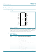
TFA9810 NXP Semiconductors Audio amplifier 2 x 12 W 7. Pinning information 7.1 Pinning VSSD(HW) 1 IN1P 2 32 VSSD(HW) 31 STAB1 IN1N 3 VDDA1 4 30 VSSP1 29 BOOT1N VSSA1 5 28 OUT1N SO/OL 6 27 BOOT1P ENABLE 7 26 OUT1P CDELAY 8 n.c. 9 TFA9810 SO32 25 VDDP1 24 VDDP2 DIAG 10 23 OUT2P TEST 11 22 BOOT2P VSSA2 12 21 OUT2N VDDA2 13 20 BOOT2N IN2N 14 19 VSSP2 18 STAB2 IN2P 15 17 VSSD(HW) VSSD(HW) 16 010aaa017 Fig 2. Pin configuration The SO32 package has four corner leads.
TFA9810 NXP Semiconductors Audio amplifier 2 x 12 W Table 3.
TFA9810 NXP Semiconductors Audio amplifier 2 x 12 W In SLEEP mode the TFA9810 is not biased and has a very low supply current. When the TFA9810 is set to OPERATING mode the device is started via the start-up sequence, which provides a pop-free start-up behavior. After start-up the reference voltages STAB are present and the outputs start switching. Table 5. Start-up Interfacing ENABLE [V] Mode ENABLE < 0.8 V SLEEP ENABLE > 3 V OPERATING 8.
TFA9810 NXP Semiconductors Audio amplifier 2 x 12 W • OverVoltage Protection (OVP) When the supply voltage applied to the TFA9810 exceeds the maximum supply voltage threshold level the device will shut down. The device will restart when the supply voltage is within the operating range. • UnderVoltage Protection (UVP) When the supply voltage applied to the TFA9810 falls below the minimum supply voltage threshold level the device will shut down.
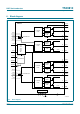
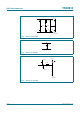
TFA9810 NXP Semiconductors Audio amplifier 2 x 12 W 8.6 Start-up sequence VP ENABLE STAB1 CDELAY V IN x FLOATING FLOATING PWM PWM AUDIO AUDIO OUT x AUDIO DIAG SLEEP START-UP OPERATING FAULT RESTART OPERATING SHUT-DOWN SLEEP 010aaa018 Fig 3. Start-up sequence 9. Internal circuitry 1,16, 17, 32 VDDA 22 V VSSA 010aaa024 Fig 4. Internal circuitry 0001 TFA9810_3 Product data sheet © NXP B.V. 2008. All rights reserved. Rev.
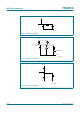
TFA9810 NXP Semiconductors Audio amplifier 2 x 12 W VDDA1 2 135 kΩ 5.5 V VSSA hvp 135 kΩ 5.5 V 3 VSSA1 010aaa025 Fig 5. Internal circuitry 0002 4 22 V 5 010aaa026 Fig 6. Internal circuitry 0003 VDDA1 VDDA1 50 µA 110 kΩ 6 VSSA1 VSSA 010aaa027 Fig 7. Internal circuitry 0004 TFA9810_3 Product data sheet © NXP B.V. 2008. All rights reserved. Rev.
TFA9810 NXP Semiconductors Audio amplifier 2 x 12 W VDDA1 3 kΩ 7 250 nA VSSA 010aaa028 Fig 8. Internal circuitry 0005 VDDA1 2 nA 8 200 nA 5 kΩ DISCHARGE VSSA1 010aaa029 Fig 9. Internal circuitry 0006 VDDA1 10 VSSA1 VSSD 010aaa030 Fig 10. Internal circuitry 0007 TFA9810_3 Product data sheet © NXP B.V. 2008. All rights reserved. Rev.
TFA9810 NXP Semiconductors Audio amplifier 2 x 12 W VDDA1 11 13 kΩ VSSA1 010aaa031 Fig 11. Internal circuitry 0008 Fig 12. Internal circuitry 0009 VDDA2 14 5.5 V 130 kΩ hvp VSSA2 130 kΩ 5.5 V 15 VSSA2 010aaa033 Fig 13. Internal circuitry 0010 VDDA2 100 mA 18 12 V VSSD 010aaa034 Fig 14. Internal circuitry 0011 TFA9810_3 Product data sheet © NXP B.V. 2008. All rights reserved. Rev.
TFA9810 NXP Semiconductors Audio amplifier 2 x 12 W 24 23.5 V 19 010aaa035 Fig 15. Internal circuitry 0012 20 12 V OUT2N 010aaa036 Fig 16. Internal circuitry 0013 VDDP2 21 VSSP2 010aaa037 Fig 17. Internal circuitry 0014 22 12 V OUT2P 010aaa038 Fig 18. Internal circuitry 0015 TFA9810_3 Product data sheet © NXP B.V. 2008. All rights reserved. Rev.
TFA9810 NXP Semiconductors Audio amplifier 2 x 12 W VDDP2 23 VSSP2 010aaa039 Fig 19. Internal circuitry 0016 25 23.5 V 30 010aaa040 Fig 20. Internal circuitry 0017 VDDP1 26 VSSP1 010aaa041 Fig 21. Internal circuitry 0018 Fig 22. Internal circuitry 0019 TFA9810_3 Product data sheet © NXP B.V. 2008. All rights reserved. Rev.
TFA9810 NXP Semiconductors Audio amplifier 2 x 12 W VDDP1 28 VSSP1 010aaa043 Fig 23. Internal circuitry 0020 29 12 V OUT1N 010aaa044 Fig 24. Internal circuitry 0021 VDDA1 100 mA 31 12 V VSSD 010aaa045 Fig 25. Internal circuitry 0022 10. Limiting values Table 7. Limiting values In accordance with the Absolute Maximum Rating System (IEC 60134). Symbol Parameter Conditions Min Max Unit asymmetrical −0.
TFA9810 NXP Semiconductors Audio amplifier 2 x 12 W Table 7. Limiting values …continued In accordance with the Absolute Maximum Rating System (IEC 60134). Symbol Parameter Conditions Min Max Unit Vx DIAG VSS − 0.3 +12 V IN1P - IN1N −12 +12 V IN2P - IN2N −12 +12 V all other pins VSS − 0.3 VDD + 0.
TFA9810 NXP Semiconductors Audio amplifier 2 x 12 W Table 9. Static characteristics …continued Tamb = 25 °C; VP = 12 V; fosc = 550 kHz; Figure 33 unless otherwise specified Symbol Parameter Conditions Min Typ Max Unit II input current VI = 5 V - 1 20 µA SO/OL input VIL LOW-level input voltage with respect to VSSD - - 0.4 V VIH HIGH-level input voltage with respect to VSSD 3 4 4.
TFA9810 NXP Semiconductors Audio amplifier 2 x 12 W Table 10. Dynamic characteristics …continued Tamb = 25 °C; VP = 12 V; RL = 8 Ω; Figure 33 unless otherwise specified. Symbol Parameter Conditions Min Typ Max Unit tresp response time transition PWM output from LOW to HIGH - 60 - ns - 50 - ns - 60 - ns - 50 - ns VI = 70 mV VI = 3.3 V transition PWM output from HIGH to LOW VI = 70 mV VI = 3.
TFA9810 NXP Semiconductors Audio amplifier 2 x 12 W Table 11. AC characteristics measured in typical application …continued Tamb = 25 °C; VP = 12 V; RL = 8 Ω; fosc = 550 kHz; Figure 33 unless otherwise specified.
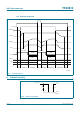
TFA9810 NXP Semiconductors Audio amplifier 2 x 12 W 010aaa019 25 Po (W) 20 (3) (2) 15 (1) 10 5 0 8 12 16 20 VP (V) (1) RL = 4 Ω (2) RL = 6 Ω (3) RL = 8 Ω Fig 26. BTL output power as function of supply voltage: THD = 0.5 %. 3 A 010aaa020 30 (3) Po (W) (2) 20 (1) 10 0 8 12 16 20 VP (V) (1) RL = 4 Ω (2) RL = 6 Ω (3) RL = 8 Ω Fig 27. BTL output power as function of supply voltage: THD = 10 %. 3 A 14.
TFA9810 NXP Semiconductors Audio amplifier 2 x 12 W • RL = load resistance [Ω]. • RDSon = drain-source on-state resistance [Ω]. • Rs = series resistance [Ω]. Example: A 4 Ω speaker in BTL configuration can be used up to a supply voltage of 12 V without running into current limiting. Current limiting (clipping) will avoid audio holes, but it causes a sound distortion similar to voltage clipping. 14.
TFA9810 NXP Semiconductors Audio amplifier 2 x 12 W OUT1P + IN1P AUDIO DSP IN1N − OUT1N 010aaa022 Fig 29. Input configuration for single-ended input 14.6 Curves measured in a typical application 010aaa197 +30 Gv (dB) +25 +20 (1) (2) +15 +10 10−2 10−1 1 102 10 fi (Hz) VP = 12 V, Vi = 100 mV (1) OUT1 (2) OUT2 Fig 30. Gain as a function of frequency TFA9810_3 Product data sheet © NXP B.V. 2008. All rights reserved. Rev.
TFA9810 NXP Semiconductors Audio amplifier 2 x 12 W 010aaa195 10 THD+N (%) 1 10−1 (2) (1) 10−2 10 102 103 104 105 fi (Hz) VP = 12 V, RL = 8 Ω, Po = 1 W (1) OUT1 (2) OUT2 Fig 31. Total harmonic distortion + noise as a function of frequency 010aaa196 10 THD+N (%) 1 10−1 (1) (2) 10−2 10−2 10−1 1 10 Po (W) VP = 12 V, RL = 8 Ω, fi = 1 kHz (1) OUT1 (2) OUT2 Fig 32. Total harmonic distortion as a function of output power 14.
xxxxxxxxxxxxxxxxxxxxx xxxxxxxxxxxxxxxxxxxxxxxxxx xxxxxxx x x x xxxxxxxxxxxxxxxxxxxxxxxxxxxxxx xxxxxxxxxxxxxxxxxxx xx xx xxxxx xxxxxxxxxxxxxxxxxxxxxxxxxxx xxxxxxxxxxxxxxxxxxx xxxxxx xxxxxxxxxxxxxxxxxxxxxxxxxxxxxxxxxxx xxxxxxxxxxxx x x xxxxxxxxxxxxxxxxxxxxx xxxxxxxxxxxxxxxxxxxxxxxxxxxxxx xxxxx xxxxxxxxxxxxxxxxxxxxxxxxxxxxxxxxxxxxxxxxxxxxxxxxxx xxxxxxxx xxxxxxxxxxxxxxxxxxxxxxxxx xxxxxxxxxxxxxxxxxxxx xxx 12 V 12 V C32 220 µF 12 V L1 BEAD R3 10 Ω C33 100 nF C3 100 nF 1 2 IN1 C4 100 nF VDDA1 4 R7 R6 10
xxxxxxxxxxxxxxxxxxxxx xxxxxxxxxxxxxxxxxxxxxxxxxx xxxxxxx x x x xxxxxxxxxxxxxxxxxxxxxxxxxxxxxx xxxxxxxxxxxxxxxxxxx xx xx xxxxx xxxxxxxxxxxxxxxxxxxxxxxxxxx xxxxxxxxxxxxxxxxxxx xxxxxx xxxxxxxxxxxxxxxxxxxxxxxxxxxxxxxxxxx xxxxxxxxxxxx x x xxxxxxxxxxxxxxxxxxxxx xxxxxxxxxxxxxxxxxxxxxxxxxxxxxx xxxxx xxxxxxxxxxxxxxxxxxxxxxxxxxxxxxxxxxxxxxxxxxxxxxxxxx xxxxxxxx xxxxxxxxxxxxxxxxxxxxxxxxx xxxxxxxxxxxxxxxxxxxx xxx 12 V 12 V C32 220 µF 12 V L1 BEAD R3 10 Ω C33 100 nF C3 100 nF 1 2 IN1 ENABLE C4 100 nF GND VDDA1 R
TFA9810 NXP Semiconductors Audio amplifier 2 x 12 W 14.8 Typical application: bill of materials Table 13. Typical application: bill of materials Item Quantity Reference Part Description 1 2 C1, C2. 220 µF/35 V General purpose 85 °C, diameter 8 mm 2 5 C3, C4, C5, C31, C33. 100 nF/50 V SMD 0805 X7R 3 2 C16, C17. 1 µF/50 V SMD 1206 X7R 4 4 C6, C7, C18, C26 1 µF/25 V MKT 5 4 C8, C10, C21, C24. 220 pF/25 V SMD 0402 NP0 6 4 C9, C14, C19, C25.
TFA9810 NXP Semiconductors Audio amplifier 2 x 12 W 16. Package outline SO32: plastic small outline package; 32 leads; body width 7.5 mm SOT287-1 D E A X c y HE v M A Z 17 32 Q A2 A (A 3) A1 pin 1 index θ Lp L 16 1 0 detail X w M bp e 5 10 mm scale DIMENSIONS (inch dimensions are derived from the original mm dimensions) UNIT A max. A1 A2 A3 bp c D (1) E (1) e HE L Lp Q v w y Z (1) mm 2.65 0.3 0.1 2.45 2.25 0.25 0.49 0.36 0.27 0.18 20.7 20.3 7.6 7.4 1.
TFA9810 NXP Semiconductors Audio amplifier 2 x 12 W 17. Revision history Table 15. Revision history Document ID Release date Data sheet status Change notice Supersedes TFA9810_3 20080220 Product data sheet - TFA9810_2 Modifications: • • Figure 33 has been updated. Figure 34 has been added. TFA9810_2 20070831 Preliminary data sheet - TFA9810_1 TFA9810_1 20070815 Preliminary data sheet - - TFA9810_3 Product data sheet © NXP B.V. 2008. All rights reserved. Rev.
TFA9810 NXP Semiconductors Audio amplifier 2 x 12 W 18. Legal information 18.1 Data sheet status Document status[1][2] Product status[3] Definition Objective [short] data sheet Development This document contains data from the objective specification for product development. Preliminary [short] data sheet Qualification This document contains data from the preliminary specification. Product [short] data sheet Production This document contains the product specification.
TFA9810 NXP Semiconductors Audio amplifier 2 x 12 W 20. Contents 1 2 3 4 5 6 7 7.1 7.2 8 8.1 8.2 8.3 8.3.1 8.3.2 8.4 8.5 8.6 9 10 11 12 12.1 12.2 12.3 13 14 14.1 14.2 14.3 14.4 14.5 14.6 14.7 14.8 14.9 15 16 17 18 18.1 18.2 18.3 General description . . . . . . . . . . . . . . . . . . . . . . 1 Features . . . . . . . . . . . . . . . . . . . . . . . . . . . . . . . 1 Applications . . . . . . . . . . . . . . . . . . . . . . . . . . . . 1 Quick reference data . . . . . . . . . . . . . . . . . . . . .