
Stereo Full-Bridge Audio Amplifier Product Data Sheet

TFA9810_3 © NXP B.V. 2008. All rights reserved.
Product data sheet Rev. 03 — 20 February 2008 18 of 29
NXP Semiconductors
TFA9810
Audio amplifier 2 x 12 W
[1] Minimum value determined by R5, R10, R17, R22 equalling +1 % and R7, R14, R18, R20 equalling −1 %.
13. Quality specification
In accordance with SNW-FQ-611-E, ‘if this type is used as an audio amplifier’. The
number of the quality specification can be found in the Quality Reference Handbook. The
handbook can be ordered using the code 9398 510 63011.
14. Application information
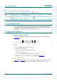
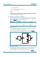
14.1 Output power estimation
For BTL configuration the output power just before clipping can be estimated using
Equation 1:
(1)
Where,
• V
P
= supply voltage (V
DDPx
− V
SSPx
) [V]
• R
L
= load resistance [Ω]
• R
DSon
= drain-source on-state resistance [Ω]
• R
s
= series resistance [Ω]
• P
o0.5 %
= output power at the THD level of 0.5 % [W]
The output power at 10 % THD can be estimated by using Equation 2:
(2)
Figure 26 and Figure 27 below show the estimated output power at THD = 0.5 % and
THD = 10 % as a function of the BLT supply voltage for different load impedances.
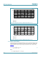
S/N signal-to-noise ratio V
o
= 10 V (RMS); gain 20 dB - 96 - dB
SVRR supply voltage ripple
rejection
V
ripple
= 2 V
(p-p)
; f
i
= 1 kHz
[1]
34 45 - dB
α
cs
channel separation P
o
= 1 W; f
i
= 1 kHz 55 70 - dB
Table 11. AC characteristics measured in typical application
…continued
T
amb
= 25
°
C; V
P
= 12 V; R
L
= 8
Ω;
f
osc
= 550 kHz; Figure 33 unless otherwise specified.
Symbol Parameter Conditions Min Typ Max Unit
BTL : P
o0.5 %
R
L
R
L
2+ R
DSon
R
s
+()×
------------------------------------------------------
V
P
×
2
2R
L
×
---------------------------------------------------------------------------------
=
P
o10 %
1.25 P×
o0.5 %
=