TFA9812 BTL stereo Class-D audio amplifier with I2S input Rev. 02 — 22 January 2009 Preliminary data sheet 1. General description The TFA9812 is a high-efficiency Bridge Tied Load (BTL) stereo Class-D audio amplifier with a digital I2S audio input. It is available in a HVQFN48 package with exposed die paddle. The exposed die paddle technology enhances the thermal and electrical performances of the device. The TFA9812 features digital sound processing and audio power amplification.
TFA9812 NXP Semiconductors BTL stereo Class-D audio amplifier with I2S input n n n n n No high system clock required (PLL is able to lock on BCK) No external heat sink required 5 V tolerant digital inputs Supports dual coil inductor application Easy application and limited external components required 2.
TFA9812 NXP Semiconductors BTL stereo Class-D audio amplifier with I2S input 4. Quick reference data Table 1. Quick reference table Unless specified otherwise, VDDA = VDDP = 12 V, VSSP1 = VSSP2 = 0 V, VDDA(3V3) = VDDD(3V3) = 3.3 V, VSS1 = VSS2 = REFD = REFA = 0 V, Tamb = 25 °C, RL = 8 Ω, fi = 1 kHz, fs = 44.1 kHz, fsw = 400 kHz, 24-bit I2S input data, MCLK clock mode, typical application diagram (Figure 13).
TFA9812 NXP Semiconductors BTL stereo Class-D audio amplifier with I2S input 5. Ordering information Table 2. Ordering information Type number TFA9812HN Package Name Description Version HVQFN48 plastic thermal enhanced very thin quad flat package; no leads; 48 terminals; body 7 × 7 × 0.85 mm SOT619-8 TFA9812_2 Preliminary data sheet © NXP B.V. 2009. All rights reserved. Rev.
xxxxxxxxxxxxxxxxxxxxx xxxxxxxxxxxxxxxxxxxxxxxxxx xxxxxxx x x x xxxxxxxxxxxxxxxxxxxxxxxxxxxxxx xxxxxxxxxxxxxxxxxxx xx xx xxxxx xxxxxxxxxxxxxxxxxxxxxxxxxxx xxxxxxxxxxxxxxxxxxx xxxxxx xxxxxxxxxxxxxxxxxxxxxxxxxxxxxxxxxxx xxxxxxxxxxxx x x xxxxxxxxxxxxxxxxxxxxx xxxxxxxxxxxxxxxxxxxxxxxxxxxxxx xxxxx xxxxxxxxxxxxxxxxxxxxxxxxxxxxxxxxxxxxxxxxxxxxxxxxxx xxxxxxxx xxxxxxxxxxxxxxxxxxxxxxxxx xxxxxxxxxxxxxxxxxxxx xxx TEST1 TEST2 AVOL 43 32 7 VDDD(3V3) VDDA(3V3) 40 3 VDDA 6 15 18, 19 REGISTER ADDRESS HEX 01 PHA
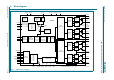
TFA9812 NXP Semiconductors BTL stereo Class-D audio amplifier with I2S input Figure 1 shows the block diagram of the TFA9812. For a detailed description of the audio signal path see Section 8.1. 7. Pinning information 37 ADSEL1/PLIM1 38 SCL/SFOR 40 VDDD(3V3) 39 SDA/MS 41 STABD 42 REFD 43 TEST2 44 DATA 45 WS 46 BCK terminal 1 index area 47 MCLK 48 VSS2 7.
TFA9812 NXP Semiconductors BTL stereo Class-D audio amplifier with I2S input Table 3.
TFA9812 NXP Semiconductors BTL stereo Class-D audio amplifier with I2S input Table 3. Pinning description TFA9812 …continued Pin Symbol Type Description 47 MCLK I/O Master clock input (I2S slave mode) or output (I2S master mode) 48 VSS2 P PCB ground reference P PCB ground reference Exposed die-paddle 8. Functional description 8.1 General The TFA9812 is a high-efficiency stereo BTL Class-D amplifier with a digital I2S audio input. It supports all commonly used I2S formats.
TFA9812 NXP Semiconductors BTL stereo Class-D audio amplifier with I2S input The block control defines the operational control settings of the TFA9812 in line with the actual I2C settings and the pin-controlled settings. The PLL block creates the system clock and can take the I2S BCK, the MCLK or an external crystal as reference source.
TFA9812 NXP Semiconductors BTL stereo Class-D audio amplifier with I2S input • In Soft mute mode the I2S input signal is overruled with a soft mute. – In Legacy control mode the analog input pin AVOL controls Soft mute mode. – In I2C control mode I2C control can be used to enable an automatic soft mute function. See also Section 8.5.3. • In Hard mute mode the PWM controller is overruled with a 50 % duty cycle square pulse. The Hard mute mode is only available in I2C control mode.
TFA9812 NXP Semiconductors BTL stereo Class-D audio amplifier with I2S input Table 6. I2S master/slave mode selection Pin value Clock mode I2S mode CSEL SDA/MS 0 0 legacy slave 0 1 legacy master - I2 C slave or master[1] 1 [1] Under these conditions the mode is enabled by the appropriate I2C setting. In I2S slave mode selection between BCK and MCLK clock modes is automatic. MCLK clock mode is given higher priority than BCK.
TFA9812 NXP Semiconductors BTL stereo Class-D audio amplifier with I2S input Table 8. Valid MCLK frequencies in I2S slave mode Control mode fs (kHz) MLCK frequency (MHz) Legacy 32 8.192 12.288 18.432 (576 fs) 44.1 11.2896 16.9344 25.4016 (576 fs) 48 12.288 18.432 27.648 (576 fs) Table 9. Valid BCK frequencies in I2S slave mode Control mode I2C Legacy [1] fs (kHz) 8 to 32 fs 8 to 192[1] 48 fs 8 to 192[1] 64 fs 32, 44.1, 48 32 fs 32, 44.1, 48 48 fs 32, 44.
TFA9812 NXP Semiconductors BTL stereo Class-D audio amplifier with I2S input 8.3 Power-up/power-down external voltage supplies POWERUP pin ENABLE pin I2C available soft mute setting in I2C mode AVOL pin in Legacy mode PWM outputs Operating mode active twake td(on) td(mute_off) td(soft_mute) 010aaa219 Fig 3. Power-up/power-down timing 8.3.1 Power-up Figure 3 and Table 10 describe the power-up timing while Table 11 shows the pin control for initiating a power-up reset. Table 10.
TFA9812 NXP Semiconductors BTL stereo Class-D audio amplifier with I2S input In I2C control mode communication is enabled after 4 ms. The preferred I2C settings can be made within 66 ms before the PLL starts running. Finally, the output stages are enabled and the audio level is increased via a demute sequence if mute has previously been disabled. Remark: In I2C mode soft mute is enabled by default. It can be disabled at any time while I2C communication is valid.
TFA9812 NXP Semiconductors BTL stereo Class-D audio amplifier with I2S input Table 12.
TFA9812 NXP Semiconductors BTL stereo Class-D audio amplifier with I2S input In I2C control mode the following sample frequency fs can be used: 8 kHz, 11.025 kHz, 12 kHz, 16 kHz, 22.05 kHz, 24 kHz, 32 kHz, 44.1 kHz, 48 kHz, 64 kHz, 88.2 kHz, 96 kHz, 128 kHz, 176.4 kHz or 192 kHz. The I2C control for fs selection can be found in Section 9.5.7. In Legacy control mode the following sample frequencies (fs) can be used: 32 kHz, 44.1 kHz or 48 kHz. 8.4.
TFA9812 NXP Semiconductors BTL stereo Class-D audio amplifier with I2S input In the above equation fc is the center frequency and fs is the sample frequency. The definition of the quality factor is the center frequency divided by the 3 dB bandwidth, see Equation 1. In parametric equalizers this is only valid when the gain is set very small (−30 dB).
TFA9812 NXP Semiconductors BTL stereo Class-D audio amplifier with I2S input K0 = G K 1 = – cos ω (5) K 2 = ( 2Q – sin ω ) ⁄ ( 2Q + sin ω ) G≥1 The ranges of the TFA9812 parametric equalizer settings for each band are: • The Gain, G is from −30 dB to +12 dB. • The center frequency, fc is from 0.0004 * fs to 0.49 * fs. • The quality factor Q is from 0.001 to 8. Using I2C control, filter coefficients need to be entered for each filter stage to configure it as desired.
TFA9812 NXP Semiconductors BTL stereo Class-D audio amplifier with I2S input 1 – k1 k1′ = 1 + k1 t1 = 1 1 – k2 k2′ = 1 + k2 t2 = 0 kx = M ⋅ 2 t1 = 0 (7) t2 = 1 –E (8) M<1 In Equation 8, M is the unsigned mantissa and E the negative signed exponent. For example, in word2 bits [14:8] = [0111 010] represent k2' = (7/24) × 2−2 = 1.09375 10−1. Table 15.
TFA9812 NXP Semiconductors BTL stereo Class-D audio amplifier with I2S input 010aaa223 12 Gain (dB) 8 4 0 101 102 103 104 105 Frequency (Hz) Fig 7. Transfer functions for several center frequencies fc 010aaa224 12 Gain (dB) 6 0 -6 -12 101 102 103 104 105 Frequency (Hz) Fig 8. Transfer functions for several gain factors G 8.5.2 Digital volume control In I2C control mode both audio channels have separate digital volume control.
TFA9812 NXP Semiconductors BTL stereo Class-D audio amplifier with I2S input Table 16. Volume control channel suppression table [7:0] control value (hexadecimal) Gain (dB) 00 0 01 −0.5 ... steps of 0.5 dB F7 −123.5 F8 −124 F9 mute Section 9 shows the I2C address locations for the digital gain control for both channels. In Legacy mode the pin AVOL (32) can be used to control the volume. Voltage levels of 0.8 V to 2.8 V correspond linearly to control values of 00h (0 dB) to F9h (mute).
TFA9812 NXP Semiconductors BTL stereo Class-D audio amplifier with I2S input Table 17. GAIN pin functionality GAIN pin value Function 0 0 dB gain 1 +24 dB gain The I2C controls for selecting the +24 dB gain can be found in Section 9.5.6. The GAIN pin has no function In I2C mode. The TFA9812 features also specific gain settings which are related to < 0.5 %, 10 %, 20 % or 30 % clipping at the output of the TFA9812.
TFA9812 NXP Semiconductors BTL stereo Class-D audio amplifier with I2S input The selected PWM switching frequency is 400 kHz by default and can be set to 350 kHz, 700 kHz and 750 kHz in I2C control mode. In Legacy mode 400 kHz is the only option and this scales linearly if 32 kHz or 48 kHz is used as fs. Remark: The selected sample frequency, fs (selected) must be equal to the sample frequency (fs) in I2C control mode.
TFA9812 NXP Semiconductors BTL stereo Class-D audio amplifier with I2S input 8.7.1 Thermal foldback If the junction temperature of the TFA9812 exceeds the programmable Thermal foldback threshold temperature the gain of the amplifier is decreased gradually to a level where the combination of dissipation (P) and the thermal resistance from junction to ambient (Rth(j-a)) results in a junction temperature around the threshold temperature.
TFA9812 NXP Semiconductors BTL stereo Class-D audio amplifier with I2S input Table 20. Undervoltage trigger levels Pin name UVP level DIAG pin (protection active) Min Max VDDA ≥7V <8V LOW VDDA(3V3) ≥ 1.6 V <3V - 8.7.6 Overdissipation protection When the output current of the power amplifiers exceeds a current value of 3 A and the temperature is above 140 °C, overdissipation protection is activated and the device enters Sleep mode.
TFA9812 NXP Semiconductors BTL stereo Class-D audio amplifier with I2S input 8.7.11 Invalid BCK protection The BCK clock signal is verified as being at one of the allowed relative frequencies: 32 fs, 48 fs or 64 fs. If it is not at one of these frequencies the TFA9812 will set the output stages to 3-state mode to prevent audible effects. The MCLK clock signal is also verified as being valid, see Section 8.2.3.
TFA9812 NXP Semiconductors BTL stereo Class-D audio amplifier with I2S input Table 21. Overview protections …continued Protections Symbol Conditions DIAG pin I2C Output flag[1] Recovering OFP PLL frequency > 140 MHz Floating OFP Floating Restart (fault to operating when PLL frequency < 140 MHz) IBP BCK/WS is not 32 ± 2, 48 2 or 64 2 - Floating Restart (fault to operating when BCK/WS is 32 ± 2, 48 2 or 64 2) Floating [1] See, Section 9.5.10.
TFA9812 NXP Semiconductors BTL stereo Class-D audio amplifier with I2S input 9.3 I2C write cycle description Table 25 shows the cycle required for writing data to the I2C registers of the TFA9812. The byte size is 8 bits. The I2C registers of the TFA9812 store two data bytes. Data is always written in pairs of two bytes. Data transfer is always MSB first. The cycle format for writing to the TFA9812 using SDA is as follows: 1. The microcontroller asserts a start condition (S). 2.
TFA9812 NXP Semiconductors BTL stereo Class-D audio amplifier with I2S input 9. The TFA9812 sends the first byte. This is the most significant byte of the register. 10. The microcontroller asserts an acknowledge. 11. The TFA9812 sends the second byte. 12. The microcontroller asserts either an acknowledge or a negative acknowledge (NA). – If the microcontroller has asserted an acknowledge, the targeted register address is auto-increased by the TFA9812 and steps 9 to 12 are repeated.
TFA9812 NXP Semiconductors BTL stereo Class-D audio amplifier with I2S input Table 27. Top-level register map …continued Register Default (hex) address (hex) Access See: Description 0x11 0x7A40 R/W Section 9.5.5 Equalizer_C2 word_2 0x12 0x14A2 R/W Section 9.5.5 Equalizer_D2 word_1 0x13 0x7A40 R/W Section 9.5.5 Equalizer_D2 word_2 0x14 0x0156 R/W Section 9.5.5 Equalizer_A3 word_1 0x15 0x4D40 R/W Section 9.5.5 Equalizer_A3 word_2 0x16 0x0156 R/W Section 9.5.
TFA9812 NXP Semiconductors BTL stereo Class-D audio amplifier with I2S input 9.5.1 Interpolator settings and soft mute Table 28. Bit Register address 00h: miscellaneous I2C interpolator settings 15 14 13 12 11 10 9 8 RSD RSD RSD RSD RSD RSD RSD RSD Default 0 0 0 0 0 0 0 0 Bit 7 6 5 4 3 2 1 0 Symbol RSD INV_POL ROFF1 ROFF0 FDEMP2 FDEMP1 FDEMP0 S_MUTE Default 0 0 1 0 0 0 0 1/0 Symbol Table 29.
TFA9812 NXP Semiconductors BTL stereo Class-D audio amplifier with I2S input Table 31. Bit description of register 00h: miscellaneous I2C interpolator settings Bit Symbol Description 15 to 8 VOL_L[15:8] See Table 16 for suppression levels on left channel as function of data byte setting. 7 to 0 VOL_R[7:0] See Table 16 for suppression levels on right channel as function of data byte setting. 9.5.3 Digital input format Table 32.
TFA9812 NXP Semiconductors BTL stereo Class-D audio amplifier with I2S input Table 35. Bit description of register 03h: equalizer configuration Bit Symbol Description 1 EQ_BP Equalizer bypass enable: 0 = Equalizer not bypassed 1 = Equalizer bypassed 0 EQ_BND Equalizer 10-band or 5-band configuration selection: 0 = 10-band equalizer configuration enabled 1 = 5-band equalizer configuration enabled 9.5.5 Equalizer settings Table 36. Register addresses xxh = 04, 06...
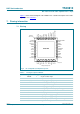
TFA9812 NXP Semiconductors BTL stereo Class-D audio amplifier with I2S input A1 Left in A2 A3 A4 A5 Left out C1 C2 C3 C4 C5 2 × 5 or 2 × 10 B1 Right in B2 B3 B4 B5 Right out D1 D2 D3 D4 D5 2 × 5 or 2 × 10 010aaa404 Fig 9. Equalizer configuration and register location mapping Table 38. Bit description of registers xxh = 04, 06...2A Bit Symbol Description 15 Eyy_t1 The filter configuration bit t1, see Section 8.5.1.2.
TFA9812 NXP Semiconductors BTL stereo Class-D audio amplifier with I2S input Table 40. Default configuration equalizer for fs = 44.1 kHz Band A1/B1 A2/B2 A3/B3 A4/B4 A5/B5 C1/D1 C2/D2 C3/D3 C4/D4 C5/D5 Frequency (Hz) 31 63 125 250 500 1000 2000 4000 8000 16000 Q-factor 1 1 1 1 1 1 1 1 1 1 Gain (dB) 0 0 0 0 0 0 0 0 0 0 9.5.6 PWM signal control Table 41.
TFA9812 NXP Semiconductors BTL stereo Class-D audio amplifier with I2S input 9.5.7 Digital-in clock configuration Table 43. Bit Register 2Dh: digital-in clock configuration 15 14 13 12 11 10 9 8 RSD RSD RSD RSD RSD RSD RSD RSD Default 0 0 0 0 0 0 0 0 Bit 7 6 5 4 3 2 1 0 Symbol RSD RSD RSD FSUB3 FSUB2 FSUB1 FSUB0 DI_MS Default 0 0 0 0 1 1 1 0 Symbol Table 44.
TFA9812 NXP Semiconductors BTL stereo Class-D audio amplifier with I2S input Table 46. Bit description of register 2Dh: digital-in clock configuration Bit Symbol Description 9 to 0 TP_THR[9:0] Reduction on the maximum temperature of 125 °C. The reduction can be calculated by: (TP_THR[9:0] reduction = INTEGER -----------------------------------in °C 2.4552 9.5.9 TFA9812 temperature Table 47.
TFA9812 NXP Semiconductors BTL stereo Class-D audio amplifier with I2S input Table 50.
TFA9812 NXP Semiconductors BTL stereo Class-D audio amplifier with I2S input Table 51. Functional control support in I2C and Legacy control modes …continued D = fixed control setting, determined by default I2C register setting; N = not supported; Y = fully supported (i.e. all options implemented in the TFA9812). Control function Reference I2C mode Legacy mode Clip level control Section 8.5.5 Y D[4] Output power limit level control Section 8.5.6 Y Y PWM signal frequency selection Section 8.5.
TFA9812 NXP Semiconductors BTL stereo Class-D audio amplifier with I2S input Table 52.
TFA9812 NXP Semiconductors BTL stereo Class-D audio amplifier with I2S input Table 52.
TFA9812 NXP Semiconductors BTL stereo Class-D audio amplifier with I2S input Table 52. Internal circuitry …continued Pin Symbol 38 SCL/SFOR Equivalent circuitry 38, 44 ESD VSS1, VSS2, REFA, REFD, Exposed die-paddle 010aaa473 39 SDA/MS 39 ESD VSS1, VSS2, REFA, REFD, Exposed die-paddle 010aaa474 45 WS 46 BCK 47 MCLK VDDD(3V3) 45, 46, 47 ESD VSS1, VSS2, REFA, REFD, Exposed die-paddle 010aaa475 11. Limiting values Table 53.
TFA9812 NXP Semiconductors BTL stereo Class-D audio amplifier with I2S input Table 53. Limiting values …continued In accordance with the Absolute Maximum Rating System (IEC 60134). Symbol Vx Parameter Conditions voltage on pin x Vesd electrostatic discharge voltage Min Max Unit DIAG [1] VSS − 0.3 VSS + 12 V POWERUP [1] VSS − 0.3 VDDA + 0.3 V ENABLE, GAIN, CSEL, ADSEL2/PLIM2, ADSEL2/PLIM1, SCL/SFOR, SDA/MS, DATA, WS, BCK, MCLK [1] VSS − 0.5 VSS + 5.5 V AVOL [1] VSS − 0.
TFA9812 NXP Semiconductors BTL stereo Class-D audio amplifier with I2S input 13. Characteristics 13.1 DC Characteristics Table 55. DC characteristics Unless specified otherwise, VDDA = VDDP = 12 V, VSSP1 = VSSP2 = 0 V, VDDA(3V3) = VDDD(3V3) = 3.3 V, VSS1 = VSS2 = REFD = REFA = 0 V, Tamb = 25 °C, RL = 8 Ω, fi = 1 kHz, fs = 44.1 kHz, fsw = 400 kHz, 24-bit I2S input data, MCLK clock mode, typical application diagram (Figure 13).
TFA9812 NXP Semiconductors BTL stereo Class-D audio amplifier with I2S input Table 55. DC characteristics …continued Unless specified otherwise, VDDA = VDDP = 12 V, VSSP1 = VSSP2 = 0 V, VDDA(3V3) = VDDD(3V3) = 3.3 V, VSS1 = VSS2 = REFD = REFA = 0 V, Tamb = 25 °C, RL = 8 Ω, fi = 1 kHz, fs = 44.1 kHz, fsw = 400 kHz, 24-bit I2S input data, MCLK clock mode, typical application diagram (Figure 13). Symbol Parameter Condition Min VOH HIGH-level output voltage At IOH = −0.
TFA9812 NXP Semiconductors BTL stereo Class-D audio amplifier with I2S input Table 55. DC characteristics …continued Unless specified otherwise, VDDA = VDDP = 12 V, VSSP1 = VSSP2 = 0 V, VDDA(3V3) = VDDD(3V3) = 3.3 V, VSS1 = VSS2 = REFD = REFA = 0 V, Tamb = 25 °C, RL = 8 Ω, fi = 1 kHz, fs = 44.1 kHz, fsw = 400 kHz, 24-bit I2S input data, MCLK clock mode, typical application diagram (Figure 13). Symbol Parameter Condition Min Typ Max Unit 118 125 132 °C - - 160 °C 20 22.
TFA9812 NXP Semiconductors BTL stereo Class-D audio amplifier with I2S input 13.2 AC characteristics Table 56. AC characteristics Unless specified otherwise, VDDA = VDDP = 12 V, VDDA(3V3) = VDDD(3V3) = 3.3 V, Tamb = 25 °C, Rs < 0.1 Ω[1], RL = 8 Ω, fi = 1 kHz, fs = 44.1 kHz, fsw = 400 kHz, 24-bit I2S input data, MCLK clock mode, typical application diagram (Figure 13). Symbol Parameter Condition Min. Typ. Max.
TFA9812 NXP Semiconductors BTL stereo Class-D audio amplifier with I2S input Table 56. AC characteristics …continued Unless specified otherwise, VDDA = VDDP = 12 V, VDDA(3V3) = VDDD(3V3) = 3.3 V, Tamb = 25 °C, Rs < 0.1 Ω[1], RL = 8 Ω, fi = 1 kHz, fs = 44.1 kHz, fsw = 400 kHz, 24-bit I2S input data, MCLK clock mode, typical application diagram (Figure 13). Symbol Parameter Condition Min. Typ. Max. Unit tPD propagation delay fs = 8 kHz - 3.6 - ms 11.025 kHz - 2.58 - ms 12 kHz - 2.
TFA9812 NXP Semiconductors BTL stereo Class-D audio amplifier with I2S input Table 57. Characteristics I2C bus interface; see Figure 10 …continued VDDD(3V3) = VDDA(3V3) = 2.7 V to 3.6 V; VDDA = VDDP = 8 V to 20 V;Tamb = −20 °C to +85 °C; all voltages referenced to ground; unless otherwise specified. Symbol Parameter tSU;STO Conditions Min Typ Max Unit set-up time for STOP condition 0.6 - - µs tBUF bus free time between a STOP and START condition 1.
TFA9812 NXP Semiconductors BTL stereo Class-D audio amplifier with I2S input δmax = Maximum duty factor (0.96). The output power at 10 % THD can be estimated using Equation 11: P O (10%) = 1.25 ⋅ P O (0.5%) (11) Figure 11 and Figure 12 show the estimated output power at THD = 0.5 % and THD = 10 % as a function of BTL supply voltage for different load impedances. 010aaa347 30 010aaa348 45 PO (10 %) W/channel PO (0.
TFA9812 NXP Semiconductors BTL stereo Class-D audio amplifier with I2S input Remark: A 4.8 Ω speaker (6 Ω speaker with 20 % spread) in BTL configuration can be used up to a supply voltage of 17 V without running into current limiting. Current limiting (clipping) will avoid audio holes, but it causes a distortion comparable to voltage clipping. 14.
xxxxxxxxxxxxxxxxxxxxx xxxxxxxxxxxxxxxxxxxxxxxxxx xxxxxxx x x x xxxxxxxxxxxxxxxxxxxxxxxxxxxxxx xxxxxxxxxxxxxxxxxxx xx xx xxxxx xxxxxxxxxxxxxxxxxxxxxxxxxxx xxxxxxxxxxxxxxxxxxx xxxxxx xxxxxxxxxxxxxxxxxxxxxxxxxxxxxxxxxxx xxxxxxxxxxxx x x xxxxxxxxxxxxxxxxxxxxx xxxxxxxxxxxxxxxxxxxxxxxxxxxxxx xxxxx xxxxxxxxxxxxxxxxxxxxxxxxxxxxxxxxxxxxxxxxxxxxxxxxxx xxxxxxxx xxxxxxxxxxxxxxxxxxxxxxxxx xxxxxxxxxxxxxxxxxxxx xxx DIAGNOSTIC NXP Semiconductors TFA9812_2 Preliminary data sheet 14.4.
xxxxxxxxxxxxxxxxxxxxx xxxxxxxxxxxxxxxxxxxxxxxxxx xxxxxxx x x x xxxxxxxxxxxxxxxxxxxxxxxxxxxxxx xxxxxxxxxxxxxxxxxxx xx xx xxxxx xxxxxxxxxxxxxxxxxxxxxxxxxxx xxxxxxxxxxxxxxxxxxx xxxxxx xxxxxxxxxxxxxxxxxxxxxxxxxxxxxxxxxxx xxxxxxxxxxxx x x xxxxxxxxxxxxxxxxxxxxx xxxxxxxxxxxxxxxxxxxxxxxxxxxxxx xxxxx xxxxxxxxxxxxxxxxxxxxxxxxxxxxxxxxxxxxxxxxxxxxxxxxxx xxxxxxxx xxxxxxxxxxxxxxxxxxxxxxxxx xxxxxxxxxxxxxxxxxxxx xxx DIAGNOSTIC NXP Semiconductors TFA9812_2 Preliminary data sheet 14.4.
xxxxxxxxxxxxxxxxxxxxx xxxxxxxxxxxxxxxxxxxxxxxxxx xxxxxxx x x x xxxxxxxxxxxxxxxxxxxxxxxxxxxxxx xxxxxxxxxxxxxxxxxxx xx xx xxxxx xxxxxxxxxxxxxxxxxxxxxxxxxxx xxxxxxxxxxxxxxxxxxx xxxxxx xxxxxxxxxxxxxxxxxxxxxxxxxxxxxxxxxxx xxxxxxxxxxxx x x xxxxxxxxxxxxxxxxxxxxx xxxxxxxxxxxxxxxxxxxxxxxxxxxxxx xxxxx xxxxxxxxxxxxxxxxxxxxxxxxxxxxxxxxxxxxxxxxxxxxxxxxxx xxxxxxxx xxxxxxxxxxxxxxxxxxxxxxxxx xxxxxxxxxxxxxxxxxxxx xxx I2S master mode and Legacy control mode DIAGNOSTIC NXP Semiconductors TFA9812_2 Preliminary data sheet
xxxxxxxxxxxxxxxxxxxxx xxxxxxxxxxxxxxxxxxxxxxxxxx xxxxxxx x x x xxxxxxxxxxxxxxxxxxxxxxxxxxxxxx xxxxxxxxxxxxxxxxxxx xx xx xxxxx xxxxxxxxxxxxxxxxxxxxxxxxxxx xxxxxxxxxxxxxxxxxxx xxxxxx xxxxxxxxxxxxxxxxxxxxxxxxxxxxxxxxxxx xxxxxxxxxxxx x x xxxxxxxxxxxxxxxxxxxxx xxxxxxxxxxxxxxxxxxxxxxxxxxxxxx xxxxx xxxxxxxxxxxxxxxxxxxxxxxxxxxxxxxxxxxxxxxxxxxxxxxxxx xxxxxxxx xxxxxxxxxxxxxxxxxxxxxxxxx xxxxxxxxxxxxxxxxxxxx xxx DIAGNOSTIC NXP Semiconductors TFA9812_2 Preliminary data sheet 14.4.
TFA9812 NXP Semiconductors BTL stereo Class-D audio amplifier with I2S input 14.5 Curves measured in typical application 010aaa480 10 010aaa481 10 THD+N (%) THD+N (%) 1 1 (2) (1) (1) 10−1 10−1 (3) (2) (3) 10−2 10−2 10−1 10 102 Po (W/channel) 1 10−2 10−2 10−1 (1) fi = 6 kHz (1) fi = 6 kHz (2) fi = 1 kHz (2) fi = 1 kHz (3) fi = 100 Hz (3) fi = 100 Hz a. VP = 12 V; RL = 2 × 6 Ω b.
TFA9812 NXP Semiconductors BTL stereo Class-D audio amplifier with I2S input 010aaa484 10 THD+N (%) THD+N (%) 1 1 10−1 10−1 10−2 10 102 103 104 105 010aaa485 10 10−2 102 10 103 104 f (Hz) 105 f (Hz) a. VP = 12 V; RL = 2 × 6 Ω; Po = 1 W b. VP = 12 V; RL = 2 × 8 Ω; Po = 1 W Fig 18. Total harmonic distortion-plus-noise as a function of frequency 010aaa486 3 010aaa487 0 G (dB) −20 G (dB) −40 1 (1) −60 (2) (1) (2) −1 −80 −100 −3 10 102 103 104 105 −120 0 0.5 1 1.
TFA9812 NXP Semiconductors BTL stereo Class-D audio amplifier with I2S input 010aaa488 0 SVRR (dB) 010aaa489 100 S/N (dB) −20 (1) 90 (2) −40 (1) 80 −60 (2) 70 −80 60 −100 102 10 103 104 105 fi (Hz) VP = 12 V; Vripple = 500 mV (RMS) reference to ground; No input signal (1) RL = 8 Ω 50 10−2 10−1 10 102 Po (W/channel) 1 VP = 15 V; 20 kHz AES17 filter (1) RL = 2 × 8 Ω (2) RL = 2 × 6 Ω (2) RL = 6 Ω Fig 21. SVRR as a function of frequency Fig 22.
TFA9812 NXP Semiconductors BTL stereo Class-D audio amplifier with I2S input 010aaa492 25 Po (W/chan.) 010aaa493 25 Po (W/chan.) 20 (1) 15 (2) (1) 15 (2) (3) (3) 10 20 10 (4) (4) 5 5 0 0 8 10 12 14 16 18 VP (V) 20 (1) Power limiter = 0 dB 8 10 12 14 16 18 20 VP (V) (1) Power limiter = 0 dB (2) Power limiter = −1.5 dB (2) Power limiter = −1.5 dB (3) Power limiter = −3 dB (3) Power limiter = −3 dB (4) Power limiter = −4.5 dB (4) Power limiter = −4.5 dB a.
TFA9812 NXP Semiconductors BTL stereo Class-D audio amplifier with I2S input 010aaa496 3 010aaa497 100 ηPO (%) P (W) (2) 80 (1) 2 (1) 60 (2) 40 1 20 0 10−2 10−1 1 0 10 102 Po (W/channel) 0 2 4 6 8 10 Po (W/channel) VP = 12 V; fi = 1 kHz; ηpo = (2 × Po) / (2 × Po + Pd) VP = 12 V; fi = 1 kHz; Power dissipation in junction only (1) RL = 2 × 6 Ω (1) RL = 2 × 6 Ω (2) RL = 2 × 8 Ω (2) RL = 2 × 8 Ω Fig 25. Power dissipation as a function of output power Fig 26.
TFA9812 NXP Semiconductors BTL stereo Class-D audio amplifier with I2S input 15. Package outline HVQFN48: plastic thermal enhanced very thin quad flat package; no leads; 48 terminals; body 7 x 7 x 0.85 mm B D SOT619-8 A terminal 1 index area E A A1 c detail X e1 e 1/2 e v w b 13 24 L M M C C A B C y1 C y 25 12 e e2 Eh 1/2 e 1 36 terminal 1 index area 48 37 X Dh 0 2.
TFA9812 NXP Semiconductors BTL stereo Class-D audio amplifier with I2S input 16. Handling information It is advisable to abide by the normal precautions appropriate to handling MOS devices. TFA9812_2 Preliminary data sheet © NXP B.V. 2009. All rights reserved. Rev.
TFA9812 NXP Semiconductors BTL stereo Class-D audio amplifier with I2S input 17. Revision history Table 59. Revision history Document ID Release date Data sheet status Change notice Supersedes TFA9812_2 20090122 Preliminary data sheet - TFA9812_1 Modifications: TFA9812_1 • Table 55 “DC characteristics” VIH maximum value updated. 2008/10/30 Preliminary data sheet TFA9812_2 Preliminary data sheet - - © NXP B.V. 2009. All rights reserved. Rev.
TFA9812 NXP Semiconductors BTL stereo Class-D audio amplifier with I2S input 18. Legal information 18.1 Data sheet status Document status[1][2] Product status[3] Definition Objective [short] data sheet Development This document contains data from the objective specification for product development. Preliminary [short] data sheet Qualification This document contains data from the preliminary specification. Product [short] data sheet Production This document contains the product specification.
TFA9812 NXP Semiconductors BTL stereo Class-D audio amplifier with I2S input 20. Contents 1 2 2.1 2.2 2.3 3 4 5 6 7 7.1 8 8.1 8.2 8.2.1 8.2.2 8.2.3 General description . . . . . . . . . . . . . . . . . . . . . . 1 Features . . . . . . . . . . . . . . . . . . . . . . . . . . . . . . . 1 General features . . . . . . . . . . . . . . . . . . . . . . . . 1 DSP features . . . . . . . . . . . . . . . . . . . . . . . . . . 2 Audio data input interface format support. . . . . 2 Applications . . . . . . . . . . .
TFA9812 NXP Semiconductors BTL stereo Class-D audio amplifier with I2S input 18.4 19 20 Trademarks . . . . . . . . . . . . . . . . . . . . . . . . . . . 64 Contact information. . . . . . . . . . . . . . . . . . . . . 64 Contents . . . . . . . . . . . . . . . . . . . . . . . . . . . . . . 65 Please be aware that important notices concerning this document and the product(s) described herein, have been included in section ‘Legal information’. © NXP B.V. 2009. All rights reserved.