
Datasheet


2000 Jul 31 4
NXP Semiconductors Product specification
Low power audio DAC with PLL UDA1334ATS
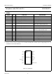
5 QUICK REFERENCE DATA
Note
1. The output voltage of the DAC scales proportionally to the power supply voltage.
SYMBOL PARAMETER CONDITIONS MIN. TYP. MAX. UNIT
Supplies
V
DDA
DAC analog supply voltage 2.4 3.0 3.6 V
V
DDD
digital supply voltage 2.4 3.0 3.6 V
I
DDA
DAC analog supply current audio mode − 3.5 − mA
video mode − 3.5 − mA
I
DDD
digital supply current audio mode − 2.5 − mA
video mode − 4.5 − mA
T
amb
ambient temperature −40 − +85 °C
Digital-to-analog converter (V
DDA
=V
DDD
=3.0V)
V
o(rms)
output voltage (RMS value) at 0 dB (FS) digital input;
note 1
− 900 − mV
(THD+N)/S total harmonic distortion-plus-noise to
signal ratio
f
s
= 44.1 kHz; at 0 dB −−90 − dB
f
s
= 44.1 kHz; at −60 dB;
A-weighted
−−40 − dB
f
s
=96kHz; at 0dB −−85 − dB
f
s
=96kHz; at −60 dB;
A-weighted
−−38 − dB
S/N signal-to-noise ratio f
s
= 44.1 kHz; code = 0;
A-weighted
− 100 − dB
f
s
=96kHz; code=0;
A-weighted
− 98 − dB
α
CS
channel separation − 100 − dB
Power dissipation (at f
s
=44.1kHz)
P power dissipation audio mode − 18 − mW
video mode − 24 − mW