
Datasheet


2000 Jul 31 6
NXP Semiconductors Product specification
Low power audio DAC with PLL UDA1334ATS
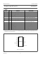
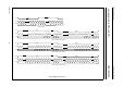
7 PINNING
Note
1. Because of test issues these pads are not 5 V tolerant and both pads should be at power supply voltage level or at
a maximum of 0.5 V above that level.
SYMBOL PIN PAD TYPE DESCRIPTION
BCK 1 5 V tolerant digital input pad bit clock input
WS 2 5 V tolerant digital input pad word select input
DATAI 3 5 V tolerant digital input pad serial data input
V
DDD
4 digital supply pad digital supply voltage
V
SSD
5 digital ground pad digital ground
SYSCLK/PLL1 6 5 V tolerant digital input pad system clock input in video mode/PLL
mode control 1 input in audio mode
SFOR1 7 5 V tolerant digital input pad serial format select 1 input
MUTE 8 5 V tolerant digital input pad mute control input
DEEM/CLKOUT 9 5 V tolerant digital input/output pad de-emphasis control input in audio
mode/clock output in video mode
PLL0 10 3-level input pad; note 1 PLL mode control 0 input
SFOR0 11 digital input pad; note 1 serial format select 0 input
V
ref(DAC)
12 analog pad DAC reference voltage
V
DDA
13 analog supply pad DAC analog supply voltage
VOUTL 14 analog output pad DAC output left
V
SSA
15 analog ground pad DAC analog ground
VOUTR 16 analog output pad DAC output right
handbook, halfpage
UDA1334ATS
MGL972
1
2
3
4
5
6
7
8
16
15
14
13
12
11
10
9
VOUTR
BCK
V
SSA
WS
VOUTL
DATAI
V
DDA
V
DDD
V
ref(DAC)
V
SSD
SFOR0SYSCLK/PLL1
PLL0SFOR1
DEEM/CLKOUTMUTE
Fig.2 Pin configuration.