
Datasheet


XC7SET02_1 © NXP B.V. 2009. All rights reserved.
Product data sheet Rev. 01 — 31 August 2009 6 of 11
NXP Semiconductors
XC7SET02
2-input NOR gate
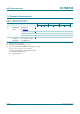
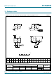
12. Waveforms
Measurement points are given in Table 9.
Fig 5. The inputs (A and B) to output (Y) propagation delays
mna106
A, B input
Y output
t
PHL
t
PLH
V
M
V
M
Table 9. Measurement point
Type Input Output
V
I
V
M
V
M
XC7SET02 GND to 3.0 V 1.5 V 0.5 × V
CC
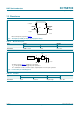
Test data is given in Table 10. Definitions for test circuit:
C
L
= Load capacitance including jig and probe capacitance.
R
T
= Termination resistance should be equal to output impedance Z
o
of the pulse generator.
Fig 6. Load circuitry for switching times
mna101
V
CC
V
I
V
O
R
T
C
L
PULSE
GENERATOR
DUT
Table 10. Test data
Type Input Load Test
V
I
t
r
, t
f
C
L
XC7SET02 3.0 V ≤ 3.0 ns 15 pF, 50 pF t
PLH
, t
PHL