
Datasheet


XC7SET125_1 © NXP B.V. 2009. All rights reserved.
Product data sheet Rev. 01 — 4 September 2009 4 of 14
NXP Semiconductors
XC7SET125
Bus buffer/line driver; 3-state
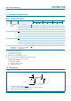
9. Recommended operating conditions
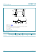
10. Static characteristics
Table 6. Recommended operating conditions
Voltages are referenced to GND (ground = 0 V).
Symbol Parameter Conditions Min Typ Max Unit
V
CC
supply voltage 4.5 5.0 5.5 V
V
I
input voltage 0 - 5.5 V
V
O
output voltage 0 - V
CC
V
T
amb
ambient temperature −40 +25 +125 °C
∆t/∆V input transition rise and fall rate - - 20 ns/V
Table 7. Static characteristics
Voltages are referenced to GND (ground = 0 V).
Symbol Parameter Conditions 25 °C −40 °C to +85 °C −40 °C to +125 °C Unit
Min Typ Max Min Max Min Max
V
IH
HIGH-level
input voltage
V
CC
= 4.5 V to 5.5 V 2.0 - - 2.0 - 2.0 - V
V
IL
LOW-level
input voltage
V
CC
= 4.5 V to 5.5 V - - 0.8 - 0.8 - 0.8 V
V
OH
HIGH-level
output voltage
V
I
= V
IH
or V
IL
; V
CC
= 4.5 V
I
O
= −50 µA 4.4 4.5 - 4.4 - 4.4 - V
I
O
= −8.0 mA 3.94 - - 3.8 - 3.70 - V
V
OL
LOW-level
output voltage
V
I
= V
IH
or V
IL
; V
CC
= 4.5 V
I
O
= 50 µA - 0 0.1 - 0.1 - 0.1 V
I
O
= 8.0 mA - - 0.36 - 0.44 - 0.55 V
I
OZ
OFF-state
output current
V
I
=V
CC
or GND;
V
CC
= 5.5 V
- - 0.25 - 2.5 - 10 µA
I
I
input leakage
current
V
I
= 5.5 V or GND;
V
CC
= 0 V to 5.5 V
- - 0.1 - 1.0 - 2.0 µA
I
CC
supply current V
I
=V
CC
or GND; I
O
= 0 A;
V
CC
= 5.5 V
- - 1.0 - 10 - 40 µA
∆I
CC
additional
supply current
per input pin; V
I
= 3.4 V;
other inputs at V
CC
or GND;
I
O
= 0 A; V
CC
= 5.5 V
- - 1.35 - 1.5 - 1.5 mA
C
I
input
capacitance
- 1.5 10 - 10 - 10 pF